Researchers at the National Institute of Standards and Technology’s (NIST) Physical Measurement Laboratory (PML), Gaithersburg, Md., have devised an idea for determining the 3D shape of features as small as 10 nm wide. The model-based method compares data from scanning electron microscope (SEM) images with stored entries in a library of 3D shapes to find a match and to determine the shape of the sample. The work provides a powerful new way to characterize nanostructures.
The SEM is widely used in various fields of industry and science because it is one of the most versatile imaging and measurement instruments. The size and shape of nanometer-scale structures are important pieces of information to know especially for manufacturing integrated circuits (ICs) and nanoscale features. The SEM, with better than 1 nm resolution, provides information on these structures that is typically interpreted as 2D images. But those images contain a wealth of information related to all three dimensions, and the PML scientists set out to capture it.
At the beginning of this work, there were two obstacles to achieving very high accuracy, one affecting the quality of measurements and the other the interpretation: (1) the image and measurement quality is degraded by drift of the sample and the electron beam, as even slight movements result in distorted images, and (2) the proper interpretation of SEM results requires an accurate, physics-based model of the relationship between the 3D sample geometry and the intensity of the signal used to acquire the images.
To surmount those obstacles, a team led by András E. Vladár of PML’s Semiconductor and Dimensional Metrology Division successfully developed a model-based measurement method that reconstructs the 3D shape and for the first time successfully applied it to 10 nm scale structures. They have developed two software programs: a fast image acquisition method that is capable of compensating for the inevitable sample and electron beam drift; and a Monte Carlo simulation-based method to interpret the 2D images in 3D.
The first software, called ACCORD, works with 2D Fourier-transforms to piece together many rapidly acquired images, in much the same way that astronomers are able to capture images of stars without blurring or other distortions. The result is a single drift-free image, a much closer-to-true representation of the sample than any image provided by traditional methods.
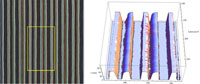
Once a good quality image is pieced together, a Monte Carlo modeling software (JMONSEL), developed by John Villarrubia of PML, is used to generate a library of SEM waveforms for 3D structures with shape parameters (e.g., widths, angles, radii of curvature) spanning a range of values around the expected ones. Narrow structures like the most recent work have 10 nm lines which place greater demands on the model because scattered electrons can emerge from several surfaces (e.g., left, right, and top) at the same time. After generating a library of SEM waveforms, the task is to identify any 3D shapes with modeled images that fit the acquired image. The result can be rendered into a 3D representation of the sample shape.
The application of these methods to SEM imaging and 3D modeling at the 10 nm level, and the quality of the results, constitute a first-in-the-world achievement. The new method is so powerful that, in this simple case of an IC structure, a single top-down image can be sufficient to determine the 3D shape along with nanometer-scale sample details.
The researchers tested their results against measurements from a transmission electron microscope (TEM) on 10 nm IC lines. The difference was less than a nanometer — as small as only a few atoms. The SEM results also matched well the results of critical dimension small angle x-ray scattering measurements.
Image –An SEM image of an IC sample of 10 nm wide SiO2 lines, with the bottom and top edges marked red and green respectively (left). The area marked with a yellow frame rendered into a 3D plot (right).
More information: