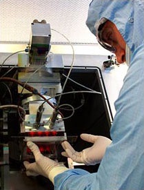
Advantech US Inc., Pittsburgh, reports that its engineers working with Penn State’s Nanofabrication Laboratory have fabricated a prototype mask of silicon etched with the required micrometer-scale features. Advantech’s evaporation process can deposit metals, dielectrics, and semiconductors using the miniLine, an in-line multi-chamber vacuum deposition system. By building up components layer by layer, Advantech is able to create complex devices with features in the size range of 3–50 micrometers.
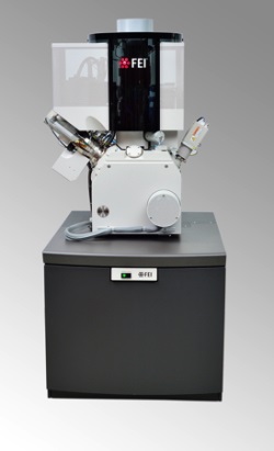
At times, however, unexpected particle contamination affects the performance of the deposited micrometer-sized electronic devices. Vince Bojan and Julie Anderson in the Materials Characterization Laboratory are using the scanning electron microscope and a scanning Auger Electron Spectrometer to identify the chemical elements in the contaminants and thus pinpoint the source of such yield-limiting defects. Together, the two labs are helping a Pennsylvania company expand into the highly competitive microelectronic devices and circuitry market with a simpler, more economical process.
Advantech Senior Scientist Volker Heydemann had this to say about working with MRI: “It’s extremely helpful to identify the chemistry of the contaminants on our products. Vince Bojan and Julie Anderson in the Materials Characterization Lab had useful results in just a couple of days. They are real experts in electron microscopy and spectroscopy. The opportunity to apply Nanofab’s processing capabilities with MCL’s advanced materials characterization techniques and expertise provides insights in our process beyond the capabilities of our in-house suite of test and quality assurance tools. Our project with Penn State helped identify and improve critical steps in our manufacturing process.”