EAG Laboratories, Tempe, Ariz., announced a new addition to its wide range of advanced microscopy techniques – Plasma FIB (PFIB) services.
PFIB can be used for both material characterization and failure analysis. It differs from traditional FIB as it uses various gases such as Xe, Ar, O, or N to generate a focused ion beam with much greater range of beam currents as compared to Ga. With Plasma FIB capability, larger cuts can be prepared more efficiently, giving EAG Laboratories the ability to survey more material to find the root cause of a failure and reducing the time needed for an analysis.
Plasma FIB Benefits:
- Higher currents and faster milling than conventional FIB
- Capable of nm to mm scale cross-sectioning with site-specific cross-sectioning up to ~1mm
- Gallium-free specific site sample preparation
- TEM, SEM and APT
- No intermetallic formation or Ga accumulation
- Multiple ion species available (Xe, Ar, O, N)
- Enables advanced characterization of Al containing materials and optoelectronics
- SEM, TEM, EELS, EDS, EBIC, CL
Plasma FIB is an ideal choice for performing mm scale targeted cross-sections on a wide variety of materials such as metals, polymers, ceramics, semiconductors and composites.
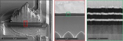
Image – Cross-Sectioning Entire Commercial LED Ball Bond.
For more information:
Evans Analytical Group