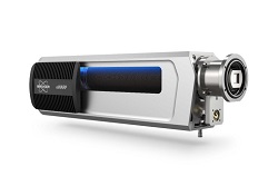
Bruker, Billerica, Mass., launched eWARP, a new detector for Electron Backscatter Diffraction (EBSD) that marks the advent of a new era in EBSD technology. Featuring a Bruker-engineered camera that combines direct electron detection and CMOS technologies, eWARP (Wide ARea Pixelated sensor) is the fastest and most signal efficient EBSD detector ever, significantly pushing the limits for materials characterization in Scanning Electron Microscopes (SEM).
Unlike other EBSD detectors in the market that use off-the-shelf sensors for direct electron detection, eWARP’s hybrid pixel sensor and high-speed signal-processing electronics are designed using a first principles approach with EBSD-specific requirements in mind. As a result, eWARP vastly outperforms existing solutions especially in terms of signal efficiency and acquisition speed, providing users with game-changing new analytical opportunities.
Combined with Bruker’s ESPRIT software suite, eWARP enables the acquisition of EBSD maps with up to 14,400 patterns per second at electron beam settings as low as 10 kV accelerating voltage and 12 nA probe current. At the core of eWARP sits the patented first ever CMOS device with on-sensor binning capability. When operated in binning mode, the sensor performs forescatter electron (FSE) and backscatter electron (BSE) imaging with up to 350,000 patterns per second.
This quantum leap in performance will have a transformational impact on the future potential of the EBSD technique, especially when it comes to challenging applications for which high spatial resolution, low electron energy and/or short exposure time are critically important. For instance:
- Automated acquisition of 3D EBSD data can now be done in much less time, at higher pixel resolution or covering a larger volume.
- The characterization of ultra-fine grained or heavily deformed materials will greatly benefit from spatial resolution improvements down to 20 nm while still operating at ultra-high speed.
- Time-resolved EBSD mapping, i.e. the acquisition of repetitive maps and images every few seconds, will become feasible, helping to understand microstructural changes inside materials during in-situ heating and/or mechanical testing experiments.
Beyond its superior analytical performance, eWARP’s design also guarantees minimized cost of ownership and maximized uptime due to remote detector monitoring for preventive/predictive maintenance, the field-replaceable camera module and user upgradable firmware for future performance and functionality improvements.
For more information:
Bruker