Skip to content

Ipsen repurposes ceramics facility for expanded hot zone production capacity

Ipsen, Pecatonica, Ill., formerly known as Ipsen Ceramics, is expanding its vacuum furnace hot zone assembly. The refurbishments include new lighting, HVAC, roofing, and other interior and exterior upgrades. Located at 325 John Street, less than 30 miles from Ipsen’s Vacuum Technology Excellence Center in Cherry Valley, the factory will initially employ up to eight material assemblers.

Incorporating the Pecatonica location into Ipsen’s vacuum furnace production and aftermarket process will provide added benefits to customers. Jake Hamid, Ipsen’s director and chief Operating Officer, stated that “Our goal is to reduce delivery times and better control the critical phase of assembly.” In the future, Ipsen is considering other manufacturing activities in Pecatonica to supplement the needs of the Vacuum Technology Excellence Center.

The move to repurpose the Pecatonica plant aligns with Ipsen’s commitment to providing high-quality vacuum furnace equipment and services to customers. The company’s dedication to meeting customer needs and reducing delivery times will be further enhanced by this strategic move, ensuring that Ipsen remains a leader in the vacuum furnace industry.

Read further here.

Veeco acquires Epiluvac AB to accelerate penetration into high growth silicon carbide epitaxy equipment market

Veeco Instruments Inc., Plainview, NY, acquired Epiluvac AB, Sweden, a privately held manufacturer of chemical vapor deposition (CVD) epitaxy systems that enable advanced silicon carbide (SiC) applications in the electric vehicle market. Epiluvac’s technology platform combined with Veeco’s global go-to-market capabilities create a significant long-term growth driver for Veeco.

The desire for clean, efficient, and reduced fossil-fuel energy is driving tremendous growth in the electric vehicle market. Applications such as on-board charging, fast charging and powertrain inverters are ideally suited for SiC power devices. The SiC device market is forecasted to grow approximately 30% compound annual growth rate (CAGR) from 2023 through 2027 according to Yole Group. Accordingly, the SiC epitaxy equipment market is expected to grow approximately 15% CAGR over the same time period according to Yole Group and internal Veeco estimates.

“The Epiluvac team has developed a superior platform and process know-how aligned with markets that are a great strategic fit for Veeco,” said Bill Miller, Veeco’s Chief Executive Officer.  “Their well-designed CVD platform achieves high productivity, is easy to maintain and has superior process control capability that make it uniquely qualified to produce devices that enable lighter, smaller and more efficient power conversion systems. We see this acquisition as a great complement to our metal organic chemical vapor deposition epitaxy product line. This acquisition accelerates our penetration into the emerging, high-growth SiC equipment market by reducing our time to market.”

“We are excited to join Veeco, a recognized leader in semiconductor and compound semiconductor capital equipment,” commented Per-Anders Eriksson, Epiluvac’s chief executive officer. “Our complementary technology platforms, along with Veeco’s extensive worldwide sales, service and manufacturing capabilities, will position us well to help our customers enable accelerated SiC adoption. The decades of research and development the Epiluvac team has invested in this demanding epitaxial process will be a great asset to Veeco’s already impressive process capabilities.”

Epiluvac is an early-stage revenue company with 11 employees. The purchase price for the transaction, all payable in cash, is $30 million paid at the time of closing with a potential additional $35 million in performance based earn-outs. The impact to Veeco’s financial results are not expected to be material in 2023 and volume revenue is expected to begin in 2024.


For more information:

Epiluvac AB

https://epiluvac.com/


Veeco

www.veeco.com


Stacking LEDs instead of placing them side by side could enable fully immersive virtual reality displays

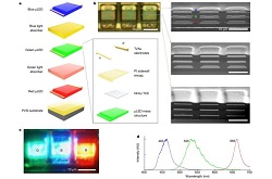
MIT engineers, Boston, Mass., have developed a new way to make sharper, defect-free displays, stacking the diodes to create vertical, multicolored pixels. Each stacked pixel can generate the full commercial range of colors and measures about 4 microns wide. The microscopic pixels, or micro-LEDs, can be packed to a density of 5,000 pixels per inch.

Over the years, the size of individual pixels has shrunk, enabling many more of them to be packed into devices to produce sharper, higher-resolution digital displays. But LEDs are reaching a limit to how small they can be while also performing effectively, especially noticeable in close-range displays such as augmented and virtual reality devices, where limited pixel density results in a “screen door effect” such that users perceive stripes in the space between pixels.

“This is the smallest micro-LED pixel, and the highest pixel density reported in the journals,” says Jeehwan Kim, associate professor of mechanical engineering at MIT. “We show that vertical pixellation is the way to go for higher-resolution displays in a smaller footprint.”

For next-generation displays, researchers are exploring inorganic micro-LEDs—diodes that are one-hundredth the size of conventional LEDs and are made from inorganic, single-crystalline semiconducting materials. Micro-LEDs could perform better, require less energy, and last longer than OLEDs.

Typical micro-LED fabrication using pick-and-place has required extreme accuracy, as microscopic pixels of red, green, and blue need to first be grown separately on wafers then precisely placed on a plate, in exact alignment with each other in order to properly reflect and produce various colors and shades. Achieving such microscopic precision is a difficult task, and entire devices need to be scrapped if pixels are found to be out of place.

The new MIT technique using vertical arrangement is an entirely different potentially less wasteful way to fabricate micro-LEDs.

The research group previously developed a method to grow and peel away perfect, two-dimensional, single-crystalline material from wafers of silicon and other surfaces—an approach they call 2D material-based layer transfer, or 2DLT.

In the current study, this approach was used to grow ultrathin membranes of red, green, and blue LEDs. They then peeled the entire LED membranes away from their base wafers, and stacked them together to make a layer cake of red, green, and blue membranes. They could then carve the cake into patterns of tiny, vertical pixels, each as small as 4 microns wide.

“In conventional displays, each R, G, and B pixel is arranged laterally, which limits how small you can create each pixel,” Shin says. “Because we are stacking all three pixels vertically, in theory we could reduce the pixel area by a third.”

The team has shown that it can grow, peel, and stack ultrathin LEDs. As a demonstration, the team fabricated a vertical LED pixel, and showed that by altering the voltage applied to each of the pixel’s red, green, and blue membranes, they could produce various colors in a single pixel.

“If you have a higher current to red, and weaker to blue, the pixel would appear pink, and so on,” Shin says. “We’re able to create all the mixed colors, and our display can cover close to the commercial color space that’s available.”

The team plans to improve the operation of the vertical pixels. So far, they have shown they can stimulate an individual structure to produce the full spectrum of colors. They will work toward making an array of many vertical micro-LED pixels.

“You need a system to control 25 million LEDs separately,” Shin says. “Here, we’ve only partially demonstrated that. The active matrix operation is something we’ll need to further develop.”

Results are published in the journal Nature.


Image – Vertically stacked, full-color µLEDs enabled by 2DLT. Courtesy of: Nature (2023).  


For more information:

Massachusetts Institute of Technology

https://web.mit.edu/

 

Steel corrosion is a major contributor to climate change

Each year, the United States spends almost a trillion dollars trying to combat metallic corrosion, an electrochemical reaction which occurs when metals oxidize and begin to rust. Now, a team of researchers led by the Ohio State University (OSU) has estimated how much corrosion is gradually worsening global carbon emissions.

Although earlier research has already estimated the economic cost of corrosion to be about three to four percent of United States’ gross domestic product, this is the first study to quantify the environmental impact associated with steel corrosion.

Global steel production has increased steadily for decades and, since steel has poor resistance to corrosion, part of that demand is to replace steel from construction materials that have become corroded over time. According to the experts, reducing the amount of steel which needs to be replaced due to corrosion could have significant effects on the amount of greenhouse gases produced to make steel.

“Given society’s reliance on coal fuel, iron and steel production is one of the largest greenhouse gases emitters of any industry. But most of the costs associated with the industry stem from the energy that goes into creating steel, and that energy is lost as the steel reverts to rust, which is like its original form of iron ore,” explained study senior author Gerald Frankel, a professor of Materials Science and Engineering at OSU.

By using historical carbon dioxide intensity data in order to estimate CO2 levels per year starting from 1960, the scientists found that, in 2021, steel production accounted for 27 percent of the carbon emissions of the global manufacturing sector, and approximately 10.5 percent of the total carbon emissions worldwide, while corroded steel emissions accounted for about 1.6 to 3.4 percent of emissions.

Fortunately, due to regulations placed on the steel industry, technological advancements in the steel industry have resulted in a 61 percent reduction in energy consumption over the past half a century. Nonetheless, policy makers and industry officials should still act urgently to amend and coordinate international policy concerning steel production and corrosion management.

“Coordinated international strategies, as well as decreasing global steel demand, by using best practices for corrosion mitigation, could better improve global corrosion management strategies and drastically reduce the rise in greenhouse gas emissions we’re seeing due to repeatedly replacing corroded steel,” Frankel said.

If such actions are not undertaken soon, greenhouse emissions caused by the steel industry could spike to 27.5 percent of the global carbon emissions by as early as 2030, with corroded steel representing four to nine percent of that number. This could have dire impacts on the Earth’s climate.

“Global warming is a societal challenge that takes coordination of a lot of multidisciplinary approaches. Our work is bringing to light an issue that seems to have gone under the radar in terms of the importance of adding to the problem,” Frankel concluded.

For more information: npj Materials Degradation