Skip to content

Wisconsin oven ships pin conveyor oven to automotive manufacturer

Wisconsin Oven Corp., East Troy, has shipped one electrically heated conveyor oven to an automotive manufacturer, which will be used for tempering automotive parts. The conveyor oven features a chain style conveyor system with vertical pins, ensuring the uniform transfer of parts through the heating and cooldown zones of the oven. The maximum temperature rating of the conveyor oven is 260° C, with interior chamber dimensions of 3’6” W x 20’10” L x 9” H.

The conveyor oven also features a top-down bottom-up airflow configuration designed with a 55,000 CFM @ 50 HP blower, ensuring optimal temperature uniformity of ±2.5° C at 163°C, documented with a temperature uniformity test. The oven is equipped with a continuous chain conveyor with vertical pins, programmable temperature controller, and recorder with Ethernet capabilities.

The unique features of this tempering oven include the ability to automatically scan the parts while being loaded onto the conveyor and validate that the correct part is being loaded, providing a pass/fail regarding heating time and temperature. The conveyor oven also includes an ambient cooldown zone and supervised installation with start-up and training.

Mike Grande, vice president of sales,said that, “Our continuous designs provide customers with innovative solutions to meet their load and process requirements. This conveyor oven was designed with high-velocity impingement air nozzles for rapid, uniform heating and optimal part results.” The equipment was fully factory tested and adjusted prior to shipment from the facility, ensuring it met all Wisconsin Oven quality standards. The equipment comes with a 2-year warranty, providing peace of mind for the automotive manufacturer.

Read further here.

Ipsen repurposes ceramics facility for expanded hot zone production capacity

Ipsen, Pecatonica, Ill., formerly known as Ipsen Ceramics, is expanding its vacuum furnace hot zone assembly. The refurbishments include new lighting, HVAC, roofing, and other interior and exterior upgrades. Located at 325 John Street, less than 30 miles from Ipsen’s Vacuum Technology Excellence Center in Cherry Valley, the factory will initially employ up to eight material assemblers.

Incorporating the Pecatonica location into Ipsen’s vacuum furnace production and aftermarket process will provide added benefits to customers. Jake Hamid, Ipsen’s director and chief Operating Officer, stated that “Our goal is to reduce delivery times and better control the critical phase of assembly.” In the future, Ipsen is considering other manufacturing activities in Pecatonica to supplement the needs of the Vacuum Technology Excellence Center.

The move to repurpose the Pecatonica plant aligns with Ipsen’s commitment to providing high-quality vacuum furnace equipment and services to customers. The company’s dedication to meeting customer needs and reducing delivery times will be further enhanced by this strategic move, ensuring that Ipsen remains a leader in the vacuum furnace industry.

Read further here.

Leading die manufacturer adds Seco/Vacuum furnace to increase capacity

Seco/Vacuum, Meadville, Pa., has announced that a U.S.-based international manufacturer has placed an order for a Vector high-pressure gas quench furnace. The new furnace will increase the partner’s heat treat capability while improving part quality. The Vector will allow the partner to heat treat larger parts, at higher quantities per cycle than their existing furnace, all with improved quality control and reliability.

The partner’s equipment requires the use of large dies that require precise heat treating. Their current heat treatment setup includes a pair of vacuum furnaces, which have some limits compared to the Vector they are about to receive.

The new furnace, a bottom loading Vector vacuum furnace with 6 bar nitrogen gas quench, has a 60″ diameter, 72″ tall, and a 3-ton capacity working zone. It is equipped with convection heating which allows them to run their tempering cycle in the same furnace without having to move parts after hardening, a tremendous time and labor savings.

The furnace is also equipped with SECO/WARWICK’s FineCarb low-pressure carburizing system for future process developments. The Vector will increase production capacity to meet the rising market demand of today and tomorrow. The new furnace’s vertical configuration and rotary hearth were built specifically to accommodate more large dies, allowing the partner to meet the elevated demand with ease. SECO/VACUUM’s intuitive process controls ensure greater heating uniformity than their existing equipment in both convection mode and in vacuum mode.

Read further here

FormFactor opens Silicon Valley Demo Center

FormFactor, Inc., Livermore, Calif., a leading semiconductor test and measurement supplier, opened a new product demonstration and training center in San Jose, California. The facility is staffed with applications engineers and training professionals, and features

FormFactor engineering wafer probers, metrology systems and advanced probe cards outfitted to meet semiconductor test and measurement requirements from lab to fab, including solutions for advanced packaging, automotive high-power devices, high-speed digital, silicon photonics, and 5G/6G/millimeter-wave mobile devices.

“The opening of our new demonstration center provides easy access for our customers to see first-hand the benefits of our sophisticated wafer probe and metrology solutions,” said Amy Leong, senior vice president and chief commercial officer. “We are deeply committed to enabling industry innovation, and proud to offer this center to accelerate our customers’ success with personalized, hands-on training, product demonstration, and support.”

FormFactor’s new demonstration center is located in the heart of Silicon Valley and offers a product demonstration lab and clean room, presentation and training areas, service warehouse, office space and conference rooms. The new location complements the capabilities of FormFactor’s existing global demonstration centers in Europe and Asia, and recently opened Advanced Quantum Cryogenic Lab in Boulder, Colorado.
For more information:

FormFactor, Inc.

www.formfactor.com

Perovskites, a ‘dirt cheap’ alternative to silicon, just got a lot more efficient

A study at the University of Rochester, Rochester, N.Y., suggests perovskites — a family of materials nicknamed for their crystalline structure that have shown extraordinary promise in recent years as a far less expensive, equally efficient replacement for silicon in solar cells and detectors — may become far more efficient.

Researchers typically synthesize perovskites in a wet lab, and then apply the material as a film on a glass substrate and explore various applications. Chunlei Guo, professor of optics at the University of Rochester leading the study reported in Nature Photonics, instead proposes a novel, physics-based approach.

By using a substrate of either a layer of metal or alternating layers of metal and dielectric material—rather than glass—he and his coauthors found they could increase the perovskite’s light conversion efficiency by 250 percent.

“No one else has come to this observation in perovskites,” Guo says. “All of a sudden, we can put a metal platform under a perovskite, utterly changing the interaction of the electrons within the perovskite. Thus, we use a physical method to engineer that interaction.”

Metals are probably the simplest materials in nature, but they can be made to acquire complex functions. The Guo Lab has extensive experience in this direction. The lab has pioneered a range of technologies transforming simple metals to pitch black, superhydrophilic (water-attracting), or superhydrophobic (water-repellent). The enhanced metals have been used for solar energy absorption and water purification in their recent studies.

In this new paper, instead of presenting a way to enhance the metal itself, the Guo Lab demonstrates how to use the metal to enhance the efficiency of pervoskites.

“A piece of metal can do just as much work as complex chemical engineering in a wet lab,” says Guo, adding that the new research may be particularly useful for future solar energy harvesting.”

In a solar cell, photons from sunlight need to interact with and excite electrons, causing the electrons to leave their atomic cores and generating an electrical current, Guo explains. Ideally, the solar cell would use materials that are weak to pull the excited electrons back to the atomic cores and stop the electrical current.

Guo’s lab demonstrated that such recombination could be substantially prevented by combining a perovskite material with either a layer of metal or a metamaterial substrate consisting of alternating layers of silver, a noble metal, and aluminum oxide, a dielectric.
The result was a significant reduction of electron recombination through “a lot of surprising physics,” Guo says. In effect, the metal layer serves as a mirror, which creates reversed images of electron-hole pairs, weakening the ability of the electrons to recombine with the holes.

The lab was able to use a simple detector to observe the resulting 250 percent increase in efficiency of light conversion.
Several challenges must be resolved before perovskites become practical for applications, especially their tendency to degrade relatively quickly. Currently, researchers are racing to find new, more stable perovskite materials.

“As new perovskites emerge, we can then use our physics-based method to further enhance their performance,” Guo says.


Image – This illustration from the Guo Lab shows the interaction between a perovskite material (cyan) and a substrate of metal-dielectric material. The red and blue pairings are electron-hole pairs. Mirror images reflected from the substrate reduce the ability of excited electrons in the perovskite to recombine with their atomic cores, increasing the efficiency of the perovskite to harvest solar light. Courtesy of: Chloe Zhang.


For more information:

University of Rochester

https://www.rochester.edu/

Raman microscope at the forefront of battery research

WITec GmbH, the originator of commercial Raman imaging systems, has delivered a new alpha300 R instrument to the Center for Solar Energy and Hydrogen Research (ZSW) Baden-Württemberg in Ulm, Germany. The Raman microscope will be used in the “Powder-Up!” pilot plant in Ulm, where cathode materials for lithium-ion batteries will be produced and the scalability of fabrication methods will be investigated.

Lithium-ion batteries are the primary enabling technology in the current shift toward electric mobility and their performance is almost exclusively determined by the materials used. ZSW is at the forefront of innovative energy storage development and is constructing a new building for the “Powder-Up!” pilot plant over the next twelve months. The new facility will focus on making improvements in the next generation of battery electrode materials, and on scaling up their manufacturing processes. This work is set to have far-reaching effects in terms of battery performance, resource use, and unit costs.

According to Dr. Margret Wohlfahrt-Mehrens, head of the Accumulators Materials Research department, “Raman microscopy is becoming a standard method in applied battery research. It quickly provides detailed information about how different electrode formulations function and degrade over charge cycles.”

WITec GmbH won the Europe-wide public tender due to the high chemical sensitivity, spatial resolution and acquisition speed of its Raman imaging systems. The alpha300 R microscope offers the added benefits of modularity for integrating hardware such as electro-chemical cells, and high sample throughput for compiling industrially relevant volumes of data.

The “Powder-Up!” facility, funded by the Baden-Württemberg Ministry of Economic Affairs, Labor and Tourism and the German Federal Ministry of Education and Research (BMBF), is the first of its kind in Europe. Material batches of up to 100 kilograms can be produced in the new plant. Such quantities are required to produce large battery cells for electric cars or stationary energy storage units.


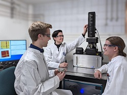
Image – Florian Klein (left) and Leon Gläser (right) from the ZSW in Ulm together with WITec Application Scientist Dr. Ievgeniia Iermak (middle) during training on the new Raman microscope.


For more information:

Oxford Instruments Group

https://www.oxinst.com

The Center for Solar Energy and Hydrogen Research Baden-Württemberg

https://www.zsw-bw.de/en.html

Exponent team receives DOE funds to advance EV battery technology

The DOE awarded $42 million in funding for 12 projects developing next-generation electric vehicle battery technologies to Exponent, Inc., Menlo Park, Calif., along with colleagues from the National Renewable Energy Laboratory (NREL) and the University of Texas, Austin. Project funding comes from the Department of Energy’s Electric Vehicles for American Low-Carbon Living (EVs4ALL) program.

“Exponent has been a leader in evaluating battery performance, risk, and safety for our clients for over 20 years,” said Ryan Spray, Ph.D., principal scientist at Exponent. “We look forward to the opportunity, with NREL and UT, to apply our deep expertise toward evaluating the energy storage technologies of tomorrow to enable new transportation possibilities.”

Deploying “clean” (zero emission) EVs is key to global decarbonization efforts. In the U.S., for instance, EVs4ALL reports that 80% adoption of EVs could reduce overall CO2 emissions by 800 million tons per year. However, the widespread adoption of EVs depends on developing more durable, faster-charging battery technologies that are effective at low temperatures.

Exponent’s team will focus on characterizing the risks posed by next-generation cells from fundamental reaction-kinetics of the materials all the way to the battery pack level. The project will lead the charge by investigating failure modes and effects, revising testing standards, and new capabilities and tools to help de-risk adoption of next-generation cells for commercial applications.


For more information:

Exponent, Inc.

https://www.exponent.com

AI-designed chips reach scale with first 100 commercial tape-outs using Synopsys technology

Synopsys, Inc., Mountain View, Calif., reaches scale for AI-driven chip designs as major semiconductor customers register the first 100 commercial tape-outs with the company’s award-winning Synopsys DSO.ai autonomous design system. Recent customers, including STMicroelectronics and SK hynix, have all seen significant uplifts in productivity and PPA, and are now charting a new design course using reinforcement learning-enabled design tools on cloud and on-premise.

By using Synopsys DSO.ai (Design Space Optimization AI) the companies are setting a blistering pace for developing advanced-node chips through the key design phases. Customers experienced more than 3x productivity increases, up to 25% lower total power, and significant reduction in die size, with reduced use of overall resources.

Traditional design space exploration has been a highly labor-intensive effort, typically requiring months of experimentation. Using AI technology, Synopsys DSO.ai searches design spaces autonomously to discover optimal PPA solutions, massively scaling the exploration of choices in chip design workflows and automating many menial tasks.

“Delivering high-performance, robust memory products at industry-leading volumes demands intensive optimization, which has traditionally been highly human intensive,” said Junhyun Chun, head of SoC (System on Chip) at SK hynix. “Synopsys DSO.ai brings a huge amount of design team efficiency, giving our engineers more time to create differentiated features for our next generation of products. It’s also driving fantastic results as demonstrated in a recent project where DSO.ai delivered a 15% cell area reduction and a 5% die shrink.”

“AI’s ability to explore broader design spaces is accelerating our customers’ relentless drive towards better PPA and higher productivity with fewer engineering resources,” said Shankar Krishnamoorthy, GM for the EDA Group at Synopsys. “We’ve monitored the first 100 commercial tape-outs by customers using Synopsys DSO.ai and the results are compelling. Whether they’re designing in the cloud, on-premise or a hybrid of the two, it’s clear that in every case, designers are seeing significant gains from optimized designs delivering better results and faster time-to-market. The cloud-side is particularly exciting as deploying Synopsys AI technology at scale in data centers ushers an exciting new era for designers everywhere.”

“Microsoft is committed to democratizing advanced chip design, so it was a natural move for us to host the Synopsys DSO.ai design system on Azure,” said Jean Boufarhat, corporate vice president, engineering, Azure Hardware and Infrastructure at Microsoft. “With AI-powered chip design on Azure, companies can leverage cloud-scaling to boost productivity and optimize very large solution spaces like high-performance computing.”


For more information:

Synopsys, Inc.

www.synopsys.com

Veeco acquires Epiluvac AB to accelerate penetration into high growth silicon carbide epitaxy equipment market

Veeco Instruments Inc., Plainview, NY, acquired Epiluvac AB, Sweden, a privately held manufacturer of chemical vapor deposition (CVD) epitaxy systems that enable advanced silicon carbide (SiC) applications in the electric vehicle market. Epiluvac’s technology platform combined with Veeco’s global go-to-market capabilities create a significant long-term growth driver for Veeco.

The desire for clean, efficient, and reduced fossil-fuel energy is driving tremendous growth in the electric vehicle market. Applications such as on-board charging, fast charging and powertrain inverters are ideally suited for SiC power devices. The SiC device market is forecasted to grow approximately 30% compound annual growth rate (CAGR) from 2023 through 2027 according to Yole Group. Accordingly, the SiC epitaxy equipment market is expected to grow approximately 15% CAGR over the same time period according to Yole Group and internal Veeco estimates.

“The Epiluvac team has developed a superior platform and process know-how aligned with markets that are a great strategic fit for Veeco,” said Bill Miller, Veeco’s Chief Executive Officer.  “Their well-designed CVD platform achieves high productivity, is easy to maintain and has superior process control capability that make it uniquely qualified to produce devices that enable lighter, smaller and more efficient power conversion systems. We see this acquisition as a great complement to our metal organic chemical vapor deposition epitaxy product line. This acquisition accelerates our penetration into the emerging, high-growth SiC equipment market by reducing our time to market.”

“We are excited to join Veeco, a recognized leader in semiconductor and compound semiconductor capital equipment,” commented Per-Anders Eriksson, Epiluvac’s chief executive officer. “Our complementary technology platforms, along with Veeco’s extensive worldwide sales, service and manufacturing capabilities, will position us well to help our customers enable accelerated SiC adoption. The decades of research and development the Epiluvac team has invested in this demanding epitaxial process will be a great asset to Veeco’s already impressive process capabilities.”

Epiluvac is an early-stage revenue company with 11 employees. The purchase price for the transaction, all payable in cash, is $30 million paid at the time of closing with a potential additional $35 million in performance based earn-outs. The impact to Veeco’s financial results are not expected to be material in 2023 and volume revenue is expected to begin in 2024.


For more information:

Epiluvac AB

https://epiluvac.com/


Veeco

www.veeco.com


Stacking LEDs instead of placing them side by side could enable fully immersive virtual reality displays

MIT engineers, Boston, Mass., have developed a new way to make sharper, defect-free displays, stacking the diodes to create vertical, multicolored pixels. Each stacked pixel can generate the full commercial range of colors and measures about 4 microns wide. The microscopic pixels, or micro-LEDs, can be packed to a density of 5,000 pixels per inch.

Over the years, the size of individual pixels has shrunk, enabling many more of them to be packed into devices to produce sharper, higher-resolution digital displays. But LEDs are reaching a limit to how small they can be while also performing effectively, especially noticeable in close-range displays such as augmented and virtual reality devices, where limited pixel density results in a “screen door effect” such that users perceive stripes in the space between pixels.

“This is the smallest micro-LED pixel, and the highest pixel density reported in the journals,” says Jeehwan Kim, associate professor of mechanical engineering at MIT. “We show that vertical pixellation is the way to go for higher-resolution displays in a smaller footprint.”

For next-generation displays, researchers are exploring inorganic micro-LEDs—diodes that are one-hundredth the size of conventional LEDs and are made from inorganic, single-crystalline semiconducting materials. Micro-LEDs could perform better, require less energy, and last longer than OLEDs.

Typical micro-LED fabrication using pick-and-place has required extreme accuracy, as microscopic pixels of red, green, and blue need to first be grown separately on wafers then precisely placed on a plate, in exact alignment with each other in order to properly reflect and produce various colors and shades. Achieving such microscopic precision is a difficult task, and entire devices need to be scrapped if pixels are found to be out of place.

The new MIT technique using vertical arrangement is an entirely different potentially less wasteful way to fabricate micro-LEDs.

The research group previously developed a method to grow and peel away perfect, two-dimensional, single-crystalline material from wafers of silicon and other surfaces—an approach they call 2D material-based layer transfer, or 2DLT.

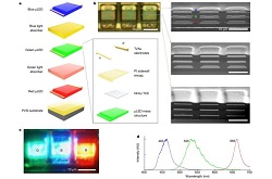
In the current study, this approach was used to grow ultrathin membranes of red, green, and blue LEDs. They then peeled the entire LED membranes away from their base wafers, and stacked them together to make a layer cake of red, green, and blue membranes. They could then carve the cake into patterns of tiny, vertical pixels, each as small as 4 microns wide.

“In conventional displays, each R, G, and B pixel is arranged laterally, which limits how small you can create each pixel,” Shin says. “Because we are stacking all three pixels vertically, in theory we could reduce the pixel area by a third.”

The team has shown that it can grow, peel, and stack ultrathin LEDs. As a demonstration, the team fabricated a vertical LED pixel, and showed that by altering the voltage applied to each of the pixel’s red, green, and blue membranes, they could produce various colors in a single pixel.

“If you have a higher current to red, and weaker to blue, the pixel would appear pink, and so on,” Shin says. “We’re able to create all the mixed colors, and our display can cover close to the commercial color space that’s available.”

The team plans to improve the operation of the vertical pixels. So far, they have shown they can stimulate an individual structure to produce the full spectrum of colors. They will work toward making an array of many vertical micro-LED pixels.

“You need a system to control 25 million LEDs separately,” Shin says. “Here, we’ve only partially demonstrated that. The active matrix operation is something we’ll need to further develop.”

Results are published in the journal Nature.


Image – Vertically stacked, full-color µLEDs enabled by 2DLT. Courtesy of: Nature (2023).  


For more information:

Massachusetts Institute of Technology

https://web.mit.edu/


AMETEK Germany inaugurates new facility in Weiterstadt

Ametek Germany, part of Ametek Inc., inaugurated a new, state-of-the-art Customer Center of Excellence in Weiterstadt, Germany, that will provide enhanced support to its customers through in-person demonstrations of Ametek innovations and solutions across major industries.

The new facility features the latest products from numerous Ametek businesses, including SPECTRO, Taylor Hobson, Solartron Metrology, Creaform, MOCON, Reichert, Atlas, Brookfield, Zygo, Dunkermotoren, EGS, Motec, Powervar, SurgeX, Precitech and TMC. Service capabilities for Ametek products will also be provided.

Ametek Germany started its operations in 1973 in Meerbusch near Düsseldorf and continues to grow. In 2015, it opened the location in Weiterstadt, and since then, increasing customer demand has required an expansion to a larger facility. This new space will serve as an Ametek hub of innovation for numerous industries including aerospace & defense, automotive, food, pharma and packaging, high precision metrology, material analyses, oil and gas, and power.

It held a private grand opening event held in January where Ametek employees were on-hand to provide customers, distributors, and partners with dynamic and interactive technology demonstrations.

“We are thrilled to take this next step in expansion to solve our valued customers’ complex challenges using Ametek’s differentiated technology solutions,” said Wiebke Rumpf, Ametek Germany Country Manager. “This Customer Center of Excellence represents a significant milestone for Ametek’s operations in Germany, and its location near Frankfurt is perfect for customer events, distributor meetings, customer demos and much more.”


For more information:

AMETEK

www.Ametek.com


Powdermet wins the Weatherhead 100 Award

Powdermet, Inc., representing the entire PMT Group of companies, has again been named to the prestigious Weatherhead 100 list of the fastest growing companies in Northeast Ohio.

Established in 1988, the Weatherhead 100 Awards are the premier celebration of Northeast Ohio’s spirit of entrepreneurship and the companies that are leading the way in Northeast Ohio. Each year this program recognizes an elite group of companies that are the best example leadership, growth and success in Northeast Ohio. Companies that make the list earn this distinction based on their growth over the last five years.

Though Powdermet has been named to the Weatherhead 100 multiple times, this year they were recognized as the second-fasted growing organization on the list. Powdermet founder and CEO Andrew Sherman noted, “We’re very proud of this distinction and thankful to all our employees who made it possible. While our subsidiary Terves had an exceptional year, we had great performances from all PMT Group companies. This was an outstanding year and we’re poised for dramatic future growth with significant investment in both facilities and equipment being implemented in 2023.”

PMT group is excited to be part of reshoring and redeveloping critical materials manufacturing in the US. Apart from being the only integrated US wrought magnesium and part producer, PMT group companies are investing aggressively into increased production, rare earth metals, magnets, specialty alloys, and energy storage materials. PMT Group and its subsidiaries Terves, Magnesium USA, Powdermet, Hybrid Materials, Cratus, Magnet Energy and CermeTech are playing an important role in developing and commercializing critical solutions that will enable America to continue to lead and set the path for other nations to follow.


For more information:

PMT Group

https://www.tervesinc.com


The answer to why Roman concrete is so durable

Researchers have spent decades trying to figure out the secret of Rome’s ultradurable ancient construction material, used in the famed Pantheon as well as aqueducts and seawalls that endured especially harsh environmental conditions. Now, a team of investigators from MIT, Harvard University, and laboratories in Italy and Switzerland, has made progress in this field, discovering ancient concrete-manufacturing strategies that incorporated several key self-healing functionalities.

For many years, researchers have assumed that the key to the ancient concrete’s durability was based on one ingredient: pozzolanic material such as volcanic ash from the area of Pozzuoli, on the Bay of Naples. This specific kind of ash was even shipped all across the vast Roman empire to be used in construction, and was described as a key ingredient for concrete in accounts by architects and historians at the time.

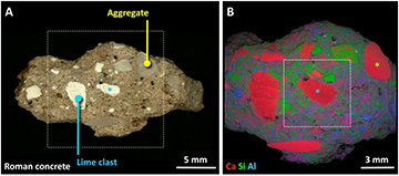
Under closer examination, these ancient samples also contain small, distinctive, millimeter-scale bright white mineral features, which have been long recognized as a ubiquitous component of Roman concretes. These white chunks, often referred to as “lime clasts,” originate from lime, another key component of the ancient concrete mix.

Upon further characterization of these lime clasts, using high-resolution multiscale imaging and chemical mapping techniques pioneered in Professor Admir Masic’s research lab at MIT, the researchers gained new insights into the potential functionality of these lime clasts.

Studying samples of this ancient concrete, he and his team determined that the white inclusions were made out of various forms of calcium carbonate. And spectroscopic examination provided clues that these had been formed at extreme temperatures, as would be expected from the exothermic reaction produced by using quicklime instead of, or in addition to, the slaked lime in the mixture. Hot mixing, the team has now concluded, was actually the key to the super-durable nature.

During the hot mixing process, the lime clasts develop a characteristically brittle nanoparticulate architecture, creating an easily fractured and reactive calcium source, which, as the team proposed, could provide a critical self-healing functionality. As soon as tiny cracks start to form within the concrete, they can preferentially travel through the high-surface-area lime clasts. This material can then react with water, creating a calcium-saturated solution, which can recrystallize as calcium carbonate and quickly fill the crack, or react with pozzolanic materials to further strengthen the composite material. These reactions take place spontaneously and therefore automatically heal the cracks before they spread. Previous support for this hypothesis was found through the examination of other Roman concrete samples that exhibited calcite-filled cracks.

To prove that this was indeed the mechanism responsible for the durability of the Roman concrete, the team produced samples of hot-mixed concrete that incorporated both ancient and modern formulations, deliberately cracked them, and then ran water through the cracks. Sure enough: Within two weeks the cracks had completely healed and the water could no longer flow. An identical chunk of concrete made without quicklime never healed, and the water just kept flowing through the sample. As a result of these successful tests, the team is working to commercialize this modified cement material.

Through the extended functional lifespan and the development of lighter-weight concrete forms, Masic hopes that these efforts could help reduce the environmental impact of cement production, which currently accounts for about 8% of global greenhouse gas emissions. Along with other new formulations, such as concrete that can actually absorb carbon dioxide from the air, another current research focus of the Masic lab, these improvements could help to reduce concrete’s global impact.

Image – Compositional and morphological characterization of ancient and modern lime clasts. (a) Optical micrographs showing the conspicuous bright white color of the lime clasts, which can easily be identified from large-area elemental mapping via SEM-EDS (b). Courtesy of Science Advances (2023). DOI: 10.1126/sciadv.add1602.

************

For more information:

Massachusetts Institute of Technology

Nupress and SPEE3D partnership brings patented cold spray technology to Australian manufacturers

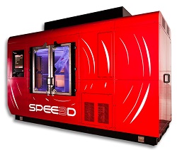
SPEE3D, Australia, announced its WarpSPEE3D printer will be hosted at Nupress headquarters in Australia. Meaning local Australian manufacturers and businesses will be able to access the machine through a subscription without having to lease or purchase it.

This unique subscription model will provide Nupress’s existing clients in the mining, building, aerospace, defense, and medical industries, and other Australian manufacturers’ access to SPEE3D’s patented cold-spray technology. It will provide them the opportunity to source parts locally and quickly from a selection of 12 different metals.

Nupress is a leading manufacturer of precision machined components and assemblies with over 50 years of expertise. Together with SPEE3D, the game-changing subscription service will enable Nupress clients and other Australian manufactures to produce parts at the time of need, rather than waiting weeks or months via other supply chains. Because metal parts can now be sourced locally, this will help manufacturing companies improve their operations and reduce costs – many of which have been impacted negatively due to ongoing global supply chain issues. The subscription model offers one to six slots, each delivering 25 hours per month of printing for 12 months.

“Democratizing access to SPEE3D’s WarpSPEED printer will help solve real-world problems around broken supply chains, manufacturing challenges, and massive delays for some of the world’s most significant industries. Local Australian companies can now access our technology thanks to Nupress, enabling smaller production runs, prototyping needs, material developments, and other advanced manufacturing capabilities,” said Steven Camilleri, Co-Founder, and CTO of SPEE3D.


Image – WarpSPEE3D, the technology that will be available at Nupress on a subscription-based service for local Australian organizations.


For more information:

Nupress

https://www.nupress.com.au/


SPEE3D

https://www.spee3d.com/


Milestone for light-driven electronics: excitons generated in a topological insulator for the first time

An international team of scientists collaborating within the Würzburg-Dresden Cluster of Excellence ct.qmat, Germany, has achieved a breakthrough in quantum research – the first detection of excitons (electrically neutral quasiparticles) in a topological insulator. This discovery paves the way for a new generation of light-driven computer chips and quantum technologies. It was enabled thanks to smart material design in Würzburg, the birthplace of topological insulators. The findings have been published in the journal Nature Communications.

In their search for novel materials for future quantum technologies, scientists from the Cluster of Excellence ct.qmat – Complexity and Topology in Quantum Matter – at the two universities in Würzburg and Dresden are concentrating on topological insulators, which enable the lossless conduction of electrical current and robust information storage. The first experimental realization of this materials class took place in Würzburg in 2007, prompting a worldwide research boom in solid-state physics that continues to this day.

Previous concepts for using topological insulators are based on the application of electrical voltages in order to control currents – an approach adopted from conventional computer chips. However, if the exotic material properties are based on electrically neutral particles (which are neither positively nor negatively charged), an electric voltage no longer works. Such quantum phenomena therefore require other tools if they are to be generated at all – for example, light.

An international research team headed by Professor Ralph Claessen, quantum physicist from Würzburg and co-spokesperson of ct.qmat, has now made a crucial discovery. “For the first time, we’ve been able to generate and experimentally detect quasiparticles known as excitons in a topological insulator. We’ve thus created a new toolkit for solid-state physics that can be used to control electrons optically.” As Claessen emphasizes, “This principle could become the basis for a new type of electronic components.”

Excitons are electronic quasiparticles. Although they seem to behave like independent particles, they actually represent an excited electronic state that can only be generated in certain types of quantum matter. “We created excitons by applying a short light pulse to a thin film consisting of just one single layer of atoms,” explains Claessen. What’s unusual about this, he says, is that the excitons were activated in a topological insulator – something that wasn’t possible before. “This has opened up a completely new line of research for topological insulators,” adds Claessen.

The right starting material is crucial – in this case bismuthene. “It’s the heavy sibling of the miracle material graphene,” says Claessen, who first tailored the topological insulator in the lab five years ago. “We’re the global leaders in this field,” he adds. “Due to our sophisticated materials design, the atoms of the single layer of bismuthene are arranged in a honeycomb pattern, just like graphene. The difference is that bismuthene’s heavy atoms make it a topological insulator, meaning it can conduct electricity along the edge without loss – even at room temperature. This can’t be done by graphene.”

For about ten years, excitons have been investigated in other two-dimensional semiconductors and regarded as information carriers for light-driven components. “For the first time, we’ve managed to optically excite excitons in a topological insulator. The interaction between light and excitons means we can expect new phenomena in such materials. This principle could be used, for example, to generate qubits,” says Claessen.

Qubits are computing units for quantum chips. They’re far superior to traditional bits and allow to solve tasks within minutes for which conventional supercomputers would literally take years.i Using light instead of electrical voltage enables quantum chips with much faster processing speeds. The latest findings therefore pave the way for future quantum technologies and a new generation of light-driven devices in microelectronics.

Image – Three excitons (pairs consisting of an electron and an electron hole) on the topological insulator bismuthene. Due to the honeycomb atomic structure, electrons can only flow along the edges. This topological effect allows current to flow without resistance. Researchers from ct.qmat have managed to generate excitons in a topological insulator for the very first time, paving the way for novel light-driven components – and possibly even the realization of qubits. Courtesy of Jörg Bandmann/ct.qmat.


For more information:

Würzburg-Dresden Cluster of Excellence ct.qmat

https://www.ctqmat.de/en


Imec enables tight standard cell boundary scaling using a two-level semi-damascene integration scheme

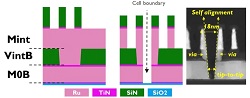
Imec, Belgium, a world-leading research and innovation hub in nanoelectronics and digital technologies, presents a semi-damascene integration approach for implementing the vertical-horizontal-vertical (VHV) scaling booster – intended to enable 4-track (4T) standard cells. The semi-damascene process enables cell boundary scaling down to 8nm tip-to-tip (T2T) in the middle-of-line (MOL) layers, providing self-aligned edges.

This provides a booster that designers can use for packing standard cells tighter, representing a 21 percent area gain over 5T designs. The novel routing scheme, along with the semi-damascene integration approach, will be critical to gradually push the logic scaling roadmap well into the Å era.

For a long time, the MOL, which provides the connection between the front-end-of-line (FEOL) and back-end-of-line (BEOL), has been organized as a single-layer contact. But currently, it is expanding into several layers, including, for example, the Mint and Vint layers. These MOL layers carry the electrical signals from the transistor’s source, drain, and gate to the local interconnects and vice versa.

Imec recently introduced a novel standard cell routing architecture called VHV, which involves the introduction of an extra MOL layer (M0B) as a scaling booster to enable 4T standard cell designs. With this booster, the first three routing layers in the standard cell follow a VHV routing style instead of the traditional HVH routing style in 5T standard cells. However, the novel two-level MOL VHV scaling booster is challenging from a process integration point of view, mainly arising from the tight boundary between neighboring 4T standard cells. The cell boundary requires a tight T2T between adjacent MOL M0B lines and two vias (VintB) facing each other with well-defined via edges – all at a minimum distance of one critical dimension (CD) of the top Mint layer. This means that the T2T and VintB via distance will need to be gradually reduced from ~24nm to ~8nm for upcoming technology nodes. This can no longer be achieved using a direct lithographic print but requires a self-aligned patterning strategy instead.

Researchers defined the tight boundary between adjacent standard cells using a two-level semi-damascene approach involving a direct metal etch. Zsolt Tőkei, program director of nano-interconnects and fellow at imec said, “Roughly speaking, we start from conventionally defined continuous lines and wider vias and, once two metal layers are finished, we split them into two, using the top 16-18nm pitch Mint layer as a hard mask for the final patterning step. This results in 3 edges (of Mint, VintB, and M0B) that are simultaneously self-aligned. With our Ru-based two-level test vehicle, we obtained an average via CD of 10.5nm and M0B T2T as tight as 8.9nm – a key achievement.” Imec researchers complemented structural validation with an initial electrical characterization of line resistance and isolation properties.

“The VHV routing scheme is a critical scaling booster to enable cell boundaries at the A10, A7, A5, A3 technology nodes,” adds Tőkei. “It also applies to future device architectures such as nanosheet, forksheet, and CFET. By extending semi-damascene from the BEOL towards the MOL, we have now also found a way to integrate this promising booster. More detailed investigations will, however, be needed, and for that purpose, imec is taping out a new dedicated mask.”


Image – (Left/middle) Schematic representation of the semi-damascene process flow used to test the key features of VHV. (Right) TEM image of the test vehicle after the final Ru etch: T2T M0B and VintB via are self-aligned to the 18mn pitch Mint layer.


For more information:

Imec

www.imec-int.com


Applied Materials launches ‘Singapore 2030’ plan to expand its operations and innovation capabilities

Applied Materials, Inc., Santa Clara, Calif., announced “Singapore 2030” – a multi-faceted plan to expand its operations in Singapore over the next eight years. The plan is targeted at strengthening the company’s global manufacturing and R&D capabilities, broadening technology ecosystem partnerships in Singapore and promoting local workforce development.

“For the past 30 years, Singapore has been a strategic hub for Applied Materials, and we are excited to build on our success with new investments that will strengthen our ability to support the semiconductor industry on its path to becoming a US$1 trillion market by the end of the decade,” said Gary Dickerson, president and CEO of Applied Materials. “We look forward to working with the Government of Singapore and the vibrant technology ecosystem to create opportunities for mutual growth that will benefit the global semiconductor industry.”

With the semiconductor industry entering a new wave of growth fueled by digital transformation of the economy, Applied has announced its intention to make multi-billion-dollar investments in its innovation infrastructure in the United States and to expand its global manufacturing capacity. As part of Singapore 2030, Applied Materials held a groundbreaking ceremony for an expansion of its regional hub in Singapore, which is home to Applied’s largest factory outside of the United States. This investment of hundreds of millions of U.S. dollars will strengthen the company’s ability to meet growing customer demand in the years ahead.

In addition, the company will invest to bolster its R&D capabilities in Singapore with a focus on accelerating commercialization of new technologies and services that improve chip power, performance, area, cost and time-to-market (PPACt). One example is the research collaboration between Applied and the Institute of Microelectronics (IME), a research institute of Singapore’s Agency for Science, Technology and Research (A*STAR), focused on hybrid bonding and other emerging, 3D chip integration technologies.

As a top employer, Applied will help enable a future-ready workforce for Singapore’s semiconductor equipment industry through enhanced training and advanced education programs. This includes an initiative with the Singapore Institute of Technology where Applied employees gain access to tailored learning modules in areas including AI and machine learning, smart manufacturing, robotics and automation, data science, and more.

Applied Materials established its presence in Singapore in 1991 with a small sales and service site that has grown to become a major manufacturing and regional operations hub with a workforce of more than 2,500. In 2019, Applied received the Distinguished Partner in Progress Award from the Government of Singapore in recognition of the company’s outstanding contributions and commitment to the country.


For more information:

Applied Materials, Inc.

www.appliedmaterials.com


Blocking radio waves and electromagnetic interference with the flip of a switch

Researchers in Drexel University’s College of Engineering have developed a thin film device fabricated by spray coating that can block electromagnetic radiation with the flip of a switch. The breakthrough, enabled by versatile two-dimensional materials called MXenes, could adjust the performance of electronic devices, strengthen wireless connections, and secure mobile communications against intrusion.

The team previously demonstrated that two-dimensional layered MXene materials – discovered just over a decade ago – when combined with an electrolyte solution, can be turned into a potent active shield against electromagnetic waves. This latest MXene discovery, reported in Nature Nanotechnology, shows how this shielding can be tuned when a small voltage – less than that produced by an alkaline battery – is applied.

MXene is a unique material in that it is highly conductive making it perfectly suited for reflecting microwave radiation that could cause static, feedback, or diminish the performance of communications devices. But its internal chemical structure can also be temporarily altered to allow these electromagnetic waves to pass through.

This means that a thin coating on a device or electrical components prevents them from both emitting electromagnetic waves, as well as being penetrated by those emitted by other electronics. Eliminating the possibility of interference from both internal and external sources can ensure the performance of the device, but some waves must be allowed to exit and enter when it is being used for communication.

The key to eliciting bidirectional tunability of MXene’s shielding property is using the flow and expulsion of ions to alternately expand and compress the space between material’s layers, like an accordion, as well as to change the surface chemistry of MXenes.

With a small voltage applied to the film, ions enter – or intercalate – between the MXene layers altering the charge of their surface and inducing electrostatic attraction, which serves to change the layer spacing, the conductivity and shielding efficiency of the material. When the ions are deintercalated as the current is switched off, the MXene layers return to their original state.

The team tested 10 different MXene-electrolyte combinations, applying each via paint sprayer in a layer about 30 to 100 times thinner than a human hair. The materials consistently demonstrated the dynamic tunability of shielding efficiency in blocking microwave radiation, which is impossible for traditional metals like copper and steel. And the device sustained the performance through more than 500 charge-discharge cycles.

These results indicate that the MXene films can convert from electromagnetic interference shielding to quasi-electromagnetic wave transmission by electrochemical oxidation of MXenes. The MXene film can potentially serve as a dynamic EMI shielding switch.
For security applications, the team suggests that the MXene shielding could hide devices from detection by radar or other tracing systems. The team also tested the potential of a one-way shielding switch. This would allow a device to remain undetectable and protected from unauthorized access until it is deployed for use.

The next step for the team is to explore additional MXene-electrolyte combinations and mechanisms to fine-tune the shielding to achieve a stronger modulation of electromagnetic wave transmission and dynamic adjustment to block radiation at a variety of bandwidths.


For more information:

Drexel University

https://drexel.edu


Chipletz selects Siemens’ EDA solutions for its smart substrate IC packaging technology

Siemens Digital Industries Software, Plano, Texas, announced that Chipletz, an innovative fabless substrate startup, has selected Siemens as its strategic electronic design automation (EDA) provider for the development of its groundbreaking Smart Substrate products.

After an extensive technical evaluation of available solutions, Chipletz selected a suite of Siemens’ industry-leading EDA tools for the design and verification of its Smart Substrate technology, which facilitates the heterogeneous integration of multiple ICs in a single package for critical artificial intelligence workloads, immersive consumer experiences, and high-performance computing.

“The Chipletz vision is to revolutionize semiconductor in-package functionality through the development of advanced packaging technology that bridges the gap between the slowing of Moore’s Law and the rising demand for compute performance,” said Bryan Black, chief executive officer of Chipletz. “Our Smart Substrate designs, now in development, are very demanding. Siemens has demonstrated that they have the ideal technology for our needs.”

To design and verify the heterogeneous integration of multiple ICs into a Smart Substrate based package, Chipletz selected Siemens’ Xpedition Substrate Integrator software, Xpedition Package Designer software, Hyperlynx software and Calibre 3DSTACK software solutions.

“Siemens is honored to be selected by Chipletz as a primary semiconductor packaging design and verification supplier,” said AJ Incorvaia, senior vice president of Electronic Board Systems at Siemens Digital Industries Software. “The Chipletz Smart Substrate technology offers Chipletz customers a robust path to bring multiple ICs, even from different vendors, into a wide range of system-in-package configurations using Siemens’ design tools to deliver a high-performing and cost-effective end-product.”


For more information:

Chipletz

https://chipletz.com/


Siemens Digital Industries Software

https://www.sw.siemens.com/en-US/


A new way to assess radiation damage in reactors

A new method could greatly reduce the time and expense needed for certain important safety checks in nuclear power reactors. The approach could save money and increase total power output in the short run, and it might increase plants’ safe operating lifetimes in the long run.

One of the most effective ways to control greenhouse gas emissions, many analysts argue, is to prolong the lifetimes of existing nuclear power plants. But extending these plants beyond their originally permitted operating lifetimes requires monitoring the condition of many of their critical components to ensure that damage from heat and radiation has not led, and will not lead, to unsafe cracking or embrittlement.

Today, testing of a reactor’s stainless-steel components — which make up much of the plumbing systems that prevent heat buildup, as well as many other parts — requires removing test pieces, known as coupons, of the same kind of steel that are left adjacent to the actual components, so they experience the same conditions. Or, it requires the removal of a tiny piece of the actual operating component. Both approaches are done during costly shutdowns of the reactor, prolonging these scheduled outages and costing millions of dollars per day.

Now, researchers at MIT and elsewhere have come up with a new, inexpensive, hands-off test that can produce similar information about the condition of these reactor components, with far less time required during a shutdown. The findings are reported today in the journal Acta Materiala in a paper by MIT professor of nuclear science and engineering Michael Short, Saleem Al Dajani a doctoral student at the King Abdullah University of Science and Technology (KAUST) in Saudi Arabia, and 13 others at MIT and other institutions.

The test involves aiming laser beams at the stainless-steel material, which generates surface acoustic waves (SAWs) on the surface. Another set of laser beams is then used to detect and measure the frequencies of these SAWs. Tests on material aged identically to nuclear power plants showed that the waves produced a distinctive double-peaked spectral signature when the material was degraded.

Short and Al Dajani embarked on the process in 2018, looking for a more rapid way to detect a specific kind of degradation, called spinodal decomposition, that can take place in austenitic stainless steel. This process can lead to embrittlement, cracking, and potential failure in the event of an emergency.

While spinodal decomposition is not the only type of degradation that can occur in reactor components, it is a primary concern for the lifetime and sustainability of nuclear reactors, Short says.

They decided to try a technique Short and his students and collaborators had expanded upon, called transient grating spectroscopy, or TGS, on samples of reactor materials known to have experienced spinodal decomposition as a result of their reactor-like thermal aging history. The method uses laser beams to stimulate, and then measure, SAWs on a material. The idea was that the decomposition should slow down the rate of heat flow through the material, that slowdown would be detectable by the TGS method.

However, it turns out there was no such slowdown. “We went in with a hypothesis about what we would see, and we were wrong,” Short says.

Instead, what showed up in the data was that, while a material would usually produce a single frequency peak for the material’s SAWs, in the degraded samples there was a splitting into two peaks.

Cast austenitic stainless steels like those used in reactor components are what’s known as duplex steels, actually a mixture of two different crystal structures in the same material by design. But while one of the two types is quite impervious to spinodal decomposition, the other is quite vulnerable to it. When the material starts to degrade, the difference shows up in the different frequency responses of the material, which is what the team found in their data.

The tests they did used large lab-based lasers and optical systems, so the next step, which the researchers are hard at work on, is miniaturizing the whole system into something that can be an easily portable test kit to use to check reactor components on-site, reducing the length of shutdowns.

Short hopes that this could help to enable the extension of power plant operating licenses for some additional decades without compromising safety, by enabling frequent, simple and inexpensive testing of the key components. Existing, large-scale plants “generate just shy of a billion dollars in carbon-free electricity per plant each year,” he says, whereas bringing a new plant online can take more than a decade. “To bridge that gap, keeping our current nukes online is the single biggest thing we can do to fight climate change.”

For more information: MIT

Researchers gain deeper understanding of mechanism behind superconductors

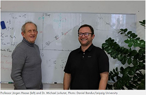
Physicists at Leipzig University have once again gained a deeper understanding of the mechanism behind superconductors. This brings the research group led by Professor Jürgen Haase one step closer to their goal of developing the foundations for a theory for superconductors that would allow current to flow without resistance and without energy loss. The researchers found that in superconducting copper-oxygen bonds, called cuprates, there must be a very specific charge distribution between the copper and the oxygen, even under pressure.
This confirmed their own findings from 2016, when Haase and his team developed an experimental method based on magnetic resonance that can measure changes that are relevant to superconductivity in the structure of materials. They were the first team in the world to identify a measurable material parameter that predicts the maximum possible transition temperature, a condition required to achieve superconductivity at room temperature. Now they have discovered that cuprates, which under pressure enhance superconductivity, follow the charge distribution predicted in 2016. The researchers have published their new findings in the journal PNAS.

“The fact that the transition temperature of cuprates can be enhanced under pressure has puzzled researchers for 30 years. But until now we didn’t know which mechanism was responsible for this,” Haase said.

He and his colleagues at the Felix Bloch Institute for Solid State Physics have now come a great deal closer to understanding the actual mechanism in these materials.

“At Leipzig University we have established the basic conditions needed to research cuprates using nuclear resonance, and Michael Jurkutat was the first doctoral researcher to join us. Together, we established the Leipzig Relation, which says that you have to take electrons away from the oxygen in these materials and give them to the copper in order to increase the transition temperature. You can do this with chemistry, but also with pressure. But hardly anyone would have thought that we could measure all of this with nuclear resonance,” Haase said.

Their current research findings could be exactly what is needed to produce a superconductor at room temperature, which has been the dream of many physicists for decades and is now expected to take only a few more years, according to Haase. To date, this has only been possible at very low temperatures around minus 150 degrees Celsius and below, which are not easy to find anywhere on Earth. About a year ago, a Canadian research group verified the findings of Professor Haase’s team from 2016 using newly developed, computer-aided calculations and thus substantiated the findings theoretically.

Superconductivity is already used today in a variety of ways, but it would be much easier and less expensive if superconductors operated at room temperature.

For more information: Leipzig University

Unlikely union of 3D-printed bronze and steel holds promise for jet engines

Skoltech researchers have used a 3D printer to fabricate samples of bronze-steel alloys previously unknown to materials science and investigated their mechanical characteristics. Blending the distinct properties of bronze and steel, the novel alloys could be used to manufacture combustion chambers for aircraft and rocket engines that would simultaneously benefit from steel’s ability to withstand extreme temperatures and bronze’s capacity to conduct heat away from the chamber and thus prevent the engine from overheating.

“3D printing is promising for manufacturing composite parts, endowed with the properties of the two distinct materials that make up the composite,” Associate Professor Igor Shishkovsky of Skoltech Materials explained. “Consider, for example, that steel is resistant to the high temperatures created by fuel combustion in an operating engine. This is great, but compared with bronze, steel is a modest thermal conductor, so the engine coolant cannot siphon heat away from it as effectively to prevent overheating and damage. Well, with 3D printing, you can actually get the best of both worlds by manufacturing a combustion chamber that seamlessly goes from being bronze on the inside for better temperature management to being steel on the outside for holding the structure together.”

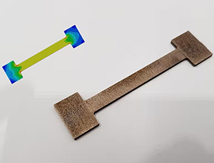
Shishkovsky was the principal investigator on the study that reported the first-ever synthesis of a bronze-steel alloy using a 3D printing technique called direct laser deposition, which melts and fuses powdered ingredients by a laser beam at every successive point in the metal part just as it’s being created. In fact, the Skoltech team combined bronze and steel in two different ways, obtaining both so-called quasi-homogeneous alloys and sandwich structures. In the former, the two materials are more or less evenly intermixed throughout the sample, while the latter consists of a series of alternating 0.25-millimeter-thick layers of bronze and steel. The researchers used one type of steel but varied its content in the alloy from 25% to 50% and experimented with three different common varieties of bronze.

The study confirmed that the two materials fused well, without defects forming, and investigated the bronze-steel alloy’s structural and mechanical properties. To do this, the team grew vertical bars from the bottom up and examined their shape, chemical composition, and microstructure.

Finding no problems at this stage, the researchers proceeded to cut out tiny pieces from different parts of the samples and investigated their internal structure with optical and scanning electron microscopy. The main mechanical characteristics were then obtained in a wide range of mechanical tests of sandwich composites continued up to their destruction. These properties are reported for the first time.

The study’s first author Konstantin Makarenko, a fourth-year Ph.D. student at Skoltech Materials, said, “Now that we have confirmed that steel and bronze can be combined in an alloy and are compatible with 3D printing via direct laser deposition, and we know the mechanical characteristics of the new material, we can explore its possible applications.  Looking forward, I would like to manufacture and test a steel-bronze combustion chamber at Skoltech, but beyond that, other items are possible and other metal combinations could be used. The next step would be to create turbine blades made of a strengthened superalloy with cooling channels made of bronze. It’s all about combining the benefits of two distinct materials in one seamless product without any welding or other junctures.”

For more information: Materials & Design