
Oxford Instruments, England, has brought together the best of its analytical innovations to form the Oxford Instruments Innovation Center, a state-of-the-art facility at its High Wycombe site.
Continue reading

Oxford Instruments, England, has brought together the best of its analytical innovations to form the Oxford Instruments Innovation Center, a state-of-the-art facility at its High Wycombe site.
Continue reading
Materials scientist Frank Mücklich, Professor of Functional Materials at Saarland University, Germany, has developed a laser surface texturing procedure that makes the surfaces of electrical contacts more stable and more efficient.
Continue reading
Thermo Fisher Scientific, Hillsboro, Ore., the world leader in serving science, introduced the Thermo Scientific Meridian EX System— an electron-beam-based failure analysis solution designed to enable precise fault localization on advanced semiconductor logic technologies that helps users localize defects within complex power networks and achieve 10X improvement in spatial resolution compared to optical fault isolation solutions.
Continue reading
Graphene, and other similar two-dimensional materials, exhibit fascinating properties such as superconductivity, extraordinary strength, and exotic quantum phenomena. Scientists at Forschungszentrum Jülich, along with partners from the Indian Institute of Technology in Patna and the Australian University of Newcastle, have now created a special material of this kind that exhibits a metallic character. It consists of just one atomic layer of molybdenum atoms and is also referred to as “molybdenene.”
The scientists succeeded in producing a thin sheet of the metal molybdenum, which is just one atomic layer thick. The new material is thus similarly thin as graphene, probably the best-known 2D material. The latter consists of carbon and was first isolated in 2004. The discovery drew great attention because graphene conducts electricity and heat far better than copper and is a hundred times more stable than steel. At the same time, it is exceptionally light and flexible. Due to its special 2D structure, graphene also exhibits some unusual electromagnetic effects that could enable groundbreaking innovations in the field of quantum technology.
In recent years, other 2D materials such as phosphorene or germanene have been introduced. Like molybdenene, they exhibit some impressive properties, while the latter still differs from other 2D materials in some aspects. “Many 2D materials are sensitive to heat, but molybdenene is not. Moreover, this is the first metallic 2D material where free-standing layers could be prepared” explains Prof. Ilia Valov from the Peter Grünberg Institute (PGI-7) at Forschungszentrum Jülich.
The researchers created the new 2D material using a microwave, in which they heated a mixture of molybdenum sulphide (MoS2) and graphene to incandescence at a temperature of around 3000°Celsius. In a reaction driven by the microwave electric field, finely branched hair structures called “whiskers” were formed. It is in the “whiskers” that the tapered molybdenum layers can be found.
In first tests, the scientists could already observe a variety of useful properties. “Molybdenene is mechanically extremely stable. It could be used, for example, as a coating for electrodes to make batteries even more powerful and robust,” explains Ilia Valov. The researchers expect that the material has further exotic electronic properties, similar to graphene, because of its special 2D structure. Due to its metallic character, it also has freely moving electrons. These accumulate on the two side sides of the molybdenene, which makes the material an interesting candidate for catalysts to accelerate chemical reactions.
In collaboration with the Indian Institute of Technology in Patna and the Australian University of Newcastle, the researchers have already been able to develop a practical scientific application for molybdenene. Thanks to its stability and excellent electrical and thermal conductivity, it is ideally suited as a measuring tip for atomic force microscopy (AFM) and surface-enhanced RAMAN spectroscopy (SERS). Initial sample recordings show that molybdenene offers various advantages over established tip materials and, because of its thin, flat shape, is capable of providing particularly good protection against unwanted interference signals.
Image – Electron microscope images of the hair-shaped structures, known as “whiskers,” which contain thin molybdenene layers. Courtesy of Nature Nanotechnology.
************
For more information:
Forschungszentrum Jülich

Testing the longevity of new electric vehicle battery designs could be four times faster with a streamlined approach, researchers at the University of Michigan have shown.
Continue readingUniversal Scientific Industrial (Shanghai) Co., Ltd., China, developed an advanced electronic component failure analysis technology to meet the increasingly complex and diverse needs of system-in-package miniaturized products.
Continue readingRigaku, Japan, leading provider of X-ray metrology solutions for semiconductor in-line processes, research and development, and high-volume manufacturing, has opened its first Semiconductor Metrology Technology Center in Sunnyvale, CA.
Continue readingAn international research group with researchers from China, Japan, and the Los Alamos National Laboratory, Los Alamos, NM, developed a new surface coating technology that is capable of significantly increasing electron emission in materials.
Continue readingResearchers at The University of Texas at Austin have discovered more than a dozen different materials for 2D semiconductors that could allow electrons to quickly move around, opening the door for a leap in electronics’ capabilities.
Continue reading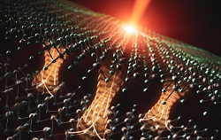 Researchers at the Department of Energy’s Lawrence Berkeley National Laboratory (Berkeley Lab), Berkeley, Calif., discover that electrons play a surprising role in heat transfer between layers of semiconductors, with implications for next-generation electronic devices.
As semiconductor devices become ever smaller, researchers are exploring two-dimensional (2D) materials for potential applications in transistors and optoelectronics. Controlling the flow of electricity and heat through these materials is key to their functionality, but first we need to understand the details of those behaviors at atomic scales.
Curious about how electrons and atomic vibrations couple to one another when heat flows between two materials, zooming into the interface with atomic precision allowed the researchers to uncover a surprisingly efficient mechanism for their coupling.
“Our work shows that we need to go beyond the analogy of Lego blocks to understand stacks of disparate 2D materials, even though the layers aren’t strongly bonded to one another,” said Archana Raja, a scientist at Berkeley Lab at who led the study. “The seemingly distinct layers, in fact, communicate through shared electronic pathways, allowing us to access and eventually design properties that are greater than the sum of the parts.”
In stacked layers of the 2D semiconductor materials tungsten diselenide (WSe2) and tungsten disulfide (WS2), researchers found that although they aren’t tightly bonded to one another, electrons provide a bridge between them that facilitates rapid heat transfer.
The devices were fabricated by Raja’s group at Berkeley Lab’s Molecular Foundry, who perfected the art of using Scotch tape to lift off crystalline monolayers of the semiconductors, each less than a nanometer in thickness. Using polymer stamps aligned under a home-built stacking microscope, these layers were deposited on top of each other and precisely placed over a microscopic window to enable the transmission of electrons through the sample.
In experiments conducted at the Department of Energy’s SLAC National Accelerator Laboratory, the team used ultrafast electron diffraction (UED) to measure the temperatures of the individual layers while optically exciting electrons in just the WSe2 layer. The UED served as an “electron camera”, capturing the atom positions within each layer. By varying the time interval between the excitation and probing pulses by trillionths of a second, they could track the changing temperature of each layer independently, using theoretical simulations to convert the observed atomic movements into temperatures.
The UED approach enables a new way of directly measuring temperature within this complex heterostructure. Aaron Lindenberg, a co-author on the study at Stanford University said “These layers are only a few angstroms apart, and yet we can selectively probe their response and, as a result of the time resolution, can probe at fundamental time scales how energy is shared between these structures in a new way.”
They found that the WSe2 layer heated up, as expected, but to their surprise, the WS2 layer also heated up in tandem, suggesting a rapid transfer of heat between layers. By contrast, when they didn’t excite electrons in the WSe2 and heated the heterostructure using a metal contact layer instead, the interface between WSe2 and WS2 transmitted heat very poorly, confirming previous reports.
“It was very surprising to see the two layers heat up almost simultaneously after photoexcitation and it motivated us to zero in on a deeper understanding of what was going on,” said Raja.
To understand their observations, the team employed theoretical calculations, using methods based on density functional theory to model how atoms and electrons behave in these systems with support from the Center for Computational Study of Excited-State Phenomena in Energy Materials (C2SEPEM), a DOE-funded Computational Materials Science Center at Berkeley Lab.
The researchers conducted extensive calculations of the electronic structure of layered 2D WSe2/WS2, as well as the behavior of lattice vibrations within the layers. Like squirrels traversing a forest canopy, who can run along paths defined by branches and occasionally jump between them, electrons in a material are limited to specific states and transitions (known as scattering), and knowledge of that electronic structure provides a guide to interpreting the experimental results.
Using computer simulations, the team explored where the electron in one layer initially wanted to scatter to, due to lattice vibrations. They found that electrons wanted to scatter to a hybrid state – a kind of ‘glue state’ where the electron hangs out in both layers at the same time. Now the team has a good idea of what these glue states look like and their signatures to confidently say that other, 2D semiconductor heterostructures will behave the same way.
The study appeared recently in Nature Nanotechnology.
Image – Artistic depiction of electron transfer driven by an ultrashort laser pulse across an interface between two atomically-thin materials. This transfer is facilitated by an interlayer ‘bridge’ state that electrons are able to access due to lattice vibrations in both materials. Courtesy of: Gregory M. Stewart/SLAC.
For more information:
Lawrence Berkeley National Laboratory
U.S. Department of Energy’s Office of Science

As electronic, thermoelectric, and computer technologies have been miniaturized to nanometer scale, engineers have faced a challenge studying fundamental properties of the materials involved; in many cases, targets are too small to be observed with optical instruments.
Using cutting-edge electron microscopes and novel techniques, a team of researchers at the University of California, Irvine, the Massachusetts Institute of Technology and other institutions has found a way to map phonons – vibrations in crystal lattices – in atomic resolution, enabling deeper understanding of the way heat travels through quantum dots, engineered nanostructures in electronic components.
To investigate how phonons are scattered by flaws and interfaces in crystals, the researchers probed the dynamic behavior of phonons near a single quantum dot of silicon-germanium using vibrational electron energy loss spectroscopy in a transmission electron microscope, equipment housed in the Irvine Materials Research Institute on the UCI campus. The results of the project are the subject of a paper published in Nature.
“We developed a novel technique to differentially map phonon momenta with atomic resolution, which enables us to observe nonequilibrium phonons that only exist near the interface,” said co-author Xiaoqing Pan, UCI professor of materials science and engineering and physics, Henry Samueli Endowed Chair in Engineering, and IMRI director.
According to Pan, at the atomic scale, heat is transported in solid materials as a wave of atoms displaced from their equilibrium position as heat moves away from the thermal source. In crystals, which possess an ordered atomic structure, these waves are called phonons: wave packets of atomic displacements that carry thermal energy equal to their frequency of vibration.
Using an alloy of silicon and germanium, the team was able to study how phonons behave in the disordered environment of the quantum dot, in the interface between the quantum dot and the surrounding silicon, and around the dome-shaped surface of the quantum dot nanostructure itself.
“We found that the SiGe alloy presented a compositionally disordered structure that impeded the efficient propagation of phonons,” said Pan. “Because silicon atoms are closer together than germanium atoms in their respective pure structures, the alloy stretches the silicon atoms a bit. Due to this strain, the UCI team discovered that phonons were being softened in the quantum dot due to the strain and alloying effect engineered within the nanostructure.”
Pan added that softened phonons have less energy, which means that each phonon carries less heat, reducing thermal conductivity as a result. The softening of vibrations is behind one of the many mechanisms of how thermoelectric devices impede the flow of heat.
Electronics engineers have succeeded in miniaturizing structures and components in electronics to such a degree that they are now down to the order of a billionth of a meter, much smaller than the wavelength of visible light, so these structures are invisible to optical techniques.
A likely field to benefit from this research is thermoelectrics – material systems that convert heat to electricity. “More than 70 percent of the energy produced by human activities is heat, so it is imperative that we find a way to recycle this back into a useable form, preferably electricity to power humanity’s increasing energy demands,” Pan said.
For more information: Nanoscale imaging of phonon dynamics by electron microscopy