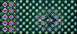
Using advanced analytical scanning transmission electron microscopy (STEM) at a magnification of 10 million times, researchers at the University of Minnesota, Minneapolis, were able to isolate and image the structure and composition of the metallic line defect in a perovskite crystal BaSnO3.
With this groundbreaking materials research, the team led by professor K. Andre Mkhoyan has made a discovery that blends the best of two sought-after qualities for touchscreens and smart windows—transparency and conductivity.
The researchers are the first to observe metallic lines in a perovskite crystal. Perovskites abound in the Earth’s center, and barium stannate (BaSnO3) is one such crystal. But, it has not been studied extensively for metallic properties because of the prevalence of more conductive materials on the planet like metals or semiconductors.
“The conductive nature and preferential direction of these metallic line defects mean we can make a material that is transparent like glass and at the same time very nicely directionally conductive like a metal,” said Mkhoyan, a TEM expert and the Ray D. and Mary T. Johnson/Mayon plastics chair in the department of chemical engineering and materials science at the University of Minnesota’s College of Science and Engineering. “This gives us the best of two worlds. We can make windows or new types of touch screens transparent and at the same time conductive. This is very exciting.”
Defects, or imperfections, are common in crystals—and line defects (the most common among them is the dislocation) are a row of atoms that deviate from the normal order. Because dislocations have the same composition of elements as the host crystal, the changes in electronic band structure at the dislocation core, due to symmetry-reduction and strain, are often only slightly different than that of the host. The researchers needed to look outside the dislocations to find the metallic line defect, where defect composition and resulting atomic structure are vastly different.
Perovskite crystals (ABX3) contain three elements in the unit cell. This gives it freedom for structural alterations such as composition and crystal symmetry, and the ability to host a variety of defects. Because of different coordination and bonding angles of the atoms in the line defect core, new electronic states are introduced and the electronic band structure is modified locally in such a dramatic way that it turns the line defect into metal.
Metallic line defects observed in MBE grown BaSnO3 films propagate along film growth direction, which means researchers can potentially control how or where line defects appear—and potentially engineer them as needed in touchscreens, smart windows, and other future technologies that demand a combination of transparency and conductivity.
Researchers verified the experimental observations of the atomic structure and electronic properties of this line defect with first principles density functional theory calculations.
The full research paper entitled “Metallic line defect in wide-bandgap transparent perovskite BaSnO3,” is published in Science Advances, a peer-reviewed scientific journal published by the American Association for the Advancement of Science.
For more information:
University of Minnesota
https://cse.umn.edu/
Science Advances
https://z.umn.edu/metallicdefect
Image – The atomic arrangement of both the BaSnO3 crystal (left) and the metallic line defect.