Scientists from the U.S. Department of Energy’s (DOE) Argonne National Laboratory, Lemont, Ill., along with three universities, have revealed new insights into the mechanism behind how gallium nitride crystals grow at the atomic scale.
Gallium nitride crystals are already in wide use in LEDs. They might also be applied to form transistors for high-power switching electronics to make electric grids more energy efficient and smarter for better balancing of high power within a system that could prevent people from losing power in severe storms or make individual homes more energy efficient. This technology could also find use in optical communications, making information transfer by lasers more precise, faster and more secure than current capabilities. Because of these diverse applications, scientists worldwide have been working to improve the process for growing gallium nitride crystals.
“Gallium nitride has a more complicated crystal structure than silicon, the typical crystalline material in electronics,” said G. Brian Stephenson, an Argonne distinguished fellow in the Materials Science division. “When you grow this crystal, you thus get more fascinating behavior at the surface.”
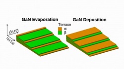
At the atomic scale, a growing gallium nitride crystal surface typically looks like a staircase of steps, where every stair is a layer of the crystal structure. Atoms are added to a growing crystal surface by attachment at the edges of the steps. Because of the gallium nitride crystal structure, the steps have alternating edge structures, labeled A and B. The different atomic structures lead to different growth behaviors of the A and B steps. Most theoretical models indicate that atoms accumulate faster on a B-type step, but experimental confirmation has been lacking.
“Because of the high temperatures and chemical atmosphere involved, it is not possible to examine the growth of gallium nitride with a standard electron microscope and test the model prediction,” Stephenson said. For that, the team called upon the Advanced Photon Source (APS), a DOE Office of Science User Facility at Argonne.
The very high energy of the x-rays available at the APS with a beam only a few micrometers wide (beamline 12-ID-D) allowed the team to monitor the rate of gallium nitride growth on the crystal surface steps. These x-rays are an ideal probe since they are sensitive to atomic-scale structure and can penetrate the environment of the crystal at growing temperatures over 1400 °F.
“Based on modeling, many had assumed that atoms probably build up faster on the type-B step,” Stephenson said. “Imagine our surprise when it turned out to be step A. This suggests the chemistry of the growth process may be more complicated than previously thought.”
The results have obvious implications for refining the current understanding of the atomic-scale mechanisms of gallium nitride growth as well as the design of advanced gallium nitride devices by allowing better control of growth and incorporation of additional elements for improved performance. The findings can also be applied to growth of related crystals, including host semiconductor materials for quantum information science.
The research was reported in Nature Communications in a paper titled “In situ microbeam surface X-ray scattering reveals alternating step kinetics during crystal growth.”
Image – Schematic of surface structures that form during gallium nitride growth processes (evaporation and deposition). The steps at the edges of each atomic layer have alternating structures (A or B). Courtesy of Argonne National Laboratory.
For more information:
Argonne National Laboratory
https://www.anl.gov/
U.S. Department of Energy’s Office of Science
https://energy.gov/science