A group of scientists led by the U.S. Department of Energy’s (DOE) Argonne National Laboratory has created a new method for improving the resolution of hard x-ray nanotomography, a noninvasive x-ray imaging technique on the scale of nanometers. The team constructed a high-resolution x-ray microscope using the powerful x-ray beams of the Advanced Photon Source (APS) and created new computer algorithms to compensate for issues encountered at tiny scales. Using this method, the team achieved a resolution below 10 nanometers.
“We want to be at 10 nanometers or better,” said Michael Wojcik, a physicist in the optics group of Argonne’s x-ray Science Division (XSD). “We developed this for nanotomography because we can obtain 3D information in the 10-nanometer range faster than other methods, but the optics and algorithm are applicable to other x-ray techniques as well.”
Using the in-house Transmission x-ray Microscope (TXM) at beamline 32-ID of the APS — including special lenses fashioned by Wojcik at the Center for Nanoscale Materials (CNM) — the team was able to use the unique characteristics of x-rays and achieve high-resolution 3D images in about an hour. But even those images were not quite at the desired resolution, so the team devised a new computer-driven technique to improve them further.
The main issues the team sought to correct are sample drift and deformation. At these small scales, if the sample moves within the beam, even by a couple nanometers, or if the x-ray beam causes even the slightest change in the sample itself, the result will be motion artifacts on the 3D image of the sample. This can make subsequent analysis much more difficult.
A sample drift can be caused by all kinds of things at that small a scale, including changes in temperature. To perform tomography, the samples also must be rotated very precisely within the beam, and that can lead to motion errors that look like sample drifts in the data. The Argonne team’s new algorithm works to remove these issues, resulting in a clearer and sharper 3D image.
“We developed an algorithm that compensates for the drift and deformation,” said Viktor Nikitin, research associate in XSD at Argonne. “When applying standard 3D reconstruction methods, we achieved a resolution in the 16 nanometer range, but with the algorithm we got it down to 10 nanometers.”
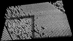
The research team tested their equipment and technique in several ways. First they captured 2D and 3D images of a tiny plate with 16-nanometer-wide features and were able to image tiny defects in the plate’s structure. They then tested it on an actual electrochemical energy storage device, using the x-rays to peer inside and capture high-resolution images.
Image – This image of a plate with 16-nanometer-wide features was captured in resolutions of less than 10 nanometers, allowing scientists to see the tiny defects in its shape. Courtesy of: Vincent De Andrade.
For more information:
Argonne National Laboratory
https://www.anl.gov/