Fujifilm Corp., Tokyo, and imec, Leuven, Belgium, developed a new photoresist technology for organic semiconductors that enables the realization of submicron patterns. Due to their lightness, flexibility, and ability to be manufactured in large area, research and development on organic semiconductors has intensified in recent years. Organic semiconductors can be used in various applications such as organic solar cells, flexible displays, organic photodetectors, and various other types of sensors.
Current methods for patterning organic semiconductors include shadow masking and inkjet printing. However, these patterning methods are not suitable for high-resolution patterning on large-size substrates. Patterning based on photolithography would solve this issue. But photolithography is currently mainly adopted for patterning of silicon semiconductors. When applying it to organic semiconductors using standard photoresists, the photoresist dissolves the organic semiconductor material during processing.
The new photoresist technology enables submicron patterning on large-size substrates without damaging the organic semiconductor materials. The technology was developed by fusing the semiconductor processing technology of Fujifilm and imec, with Fujifilm’s synthetic-organic chemistry material design technology. Because existing i-line photolithography equipment can be used, and investment for new equipment is unnecessary, the new technology contributes to a cost-effective production of high-resolution organic semiconductor devices.
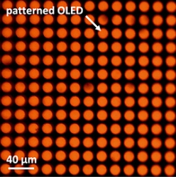
For technical verification, organic photo detectors (OPD) and organic light-emitting diodes (OLED) were developed using the new photolithography technology, and their performance was tested. Organic semiconductor materials were patterned to produce OPD composed of fine light receiving elements down to 200 × 200 μm. Generally, patterning of organic semiconductor materials degrade the property by converting light into electricity (photoelectric conversion property), but were patterned without degradation in this case. The arrays produced using the newly developed photolithography pattering method were 20 μm pitch OLEDs emitting uniform light.
Fujifilm and imec will continue to contribute to industrialization of organic electronics by advancing research and development of semiconductor materials, processing technology and system integration.
More information: