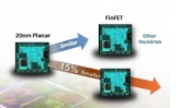
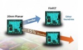
Global Foundries, Austin, Texas, and Samsung, Japan, announce a joint program for fabless companies to skip the 20nm node and move straight to 14nm FinFETs. The 14nm FinFETs offer a 20% improvement in performance and a 35% reduction in power compared to 20nm technology. The two companies offer a single process design kit (PDK) and manufacturing at four different fabs with identical processes. The single process design kit will allow customers to do a single design that is capable of being multi-sourced from different locations. The PDKs are available now, and 14nm manufacturing could move into high volume production by the end of the year.
“This is unprecedented,” said Kelvin Low, senior director of marketing at Samsung. “It never has happened in the industry, especially at the very leading edge nodes. We are confident that this will transform the supply chain model,” he added.
Fabless companies such as Qualcomm have been lobbying for such multi-sourcing for some time, and are eager to move to FinFETs that offer higher performance and reduced power consumption.
“For both Samsung and Global Foundries, we will be providing our customers with a choice and assurances of supply, enabled by the unprecedented global capacity across our respective manufacturing facilities throughout different locations worldwide,” Low said. “For Samsung, we have facilities in the U.S. in Austin. We also have a couple of plants in Korea. For Global Foundries, the 14 nm capacity will be in Malta, NY.”