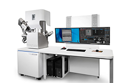
The first plasma-focused ion beam (FIB) scanning electron microscope (SEM) in Finland has just become operational at VTT in Espoo, Finland. This multi-million investment will significantly contribute to materials research for applications such as hydrogen economy, microelectronics, and the marine industry, as well as to material damage investigation.
A Tescan Amber X system, Finland’s first FIB SEM using Xenon plasma, has been taken into use at VTT Technical Research Centre of Finland. In the Nordic countries, there are just a handful of similar systems that are rare worldwide.
The multi-million priced equipment includes all the bells and whistles that a materials researcher could dream of. Compared to traditional FIB-SEMs, it provides huge potential for excelling in materials research and multiplying the speed of materials development.
Supriya Nandy, VTT senior scientist, said: “The new capability for lightning-fast materials characterization in 3D supports, for example, integrated computational materials engineering (ICME) and materials acceleration platforms (MAPs).
“While new materials traditionally take ages to develop, this capability allows us to reduce the time from design to market roughly to one-tenth.”
The new FIB-SEM is designed to perform site-specific investigations with nanometer accuracy for all types of materials, such as ceramics, metals, and even soft materials like wood and paper. The sample can be imaged and tested simultaneously, which is useful, for instance, for observing how the material reacts to a certain load.
“With the help of plasma-FIB and its in-situ testing capabilities, we can answer questions not only about the material’s properties but also about how the material behaves under strain, extreme temperatures-or both at the same time. What else could a materials scientist dream of when developing state-of-the-art materials for current and future industry needs?” Nandy continues.
The TESCAN AMBER X at VTT provides several industries with opportunities for groundbreaking materials development.
Janne Pakarinen, VTT research team leader, said: “Marine and aviation industries could benefit from our equipment to ensure their materials will always endure in various conditions. Another example is the emerging hydrogen economy, which requires careful studies and analysis of surface materials. Also, the battery and semiconductor industries could be very interested.”
In addition to the plasma-FIB, the new SEM comes with state-of-the-art detectors for energy dispersive spectroscopy (EDS) and electron back-scattering diffraction (EBSD) and in-situ tensile stage that can reach up to 1200°C.
The system has been fully operational since mid-March.
Image – Hydrogen– VTT multi-million investment in a plasma-FIB scanning electron microscope catapults Finland to the forefront of Nordic materials research.
************
For more information:
VTT Technical Research Centre of Finland Ltd.