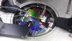
IBM, Armonk, N.Y., plans to invest $3 billion over the next five years in two broad research and early stage development programs. One such approach is graphene wafers, such as the one being tested in the image shown here. Graphene is pure carbon in the form of a one atomic-layer-thick sheet. It is an excellent conductor of heat and electricity, and it is also remarkably strong and flexible. Electrons can move in graphene about ten times faster than in commonly used semiconductor materials such as silicon and silicon germanium.
The first research program is aimed at so-called “7 nanometer and beyond” silicon technology that will address serious physical challenges that are threatening current semiconductor scaling techniques. The second is focused on developing alternative technologies for post-silicon era chips using entirely different approaches.
The “7 nanometer and beyond” silicon technology will address serious physical challenges that are threatening current semiconductor scaling techniques and will impede the ability to manufacture such chips. The second is focused on developing alternative technologies, which IBM scientists and other experts say are required because of the physical limitations of silicon-based semiconductors.
The teams will comprise IBM Research scientists and engineers from Albany and Yorktown, New York; Almaden, California; and Europe. In particular, IBM will be investing significantly in emerging areas of research that are already underway at IBM such as carbon nanoelectronics, silicon photonics, new memory technologies, and architectures that support quantum and cognitive computing.
These teams will focus on providing orders of magnitude improvement in system level performance and energy efficient computing. In addition, IBM will continue to invest in the nanosciences and quantum computing–two areas of fundamental science where IBM has remained a pioneer for over three decades.
With virtually all electronic equipment today built on complementary metal–oxide–semiconductor (CMOS) technology, there is an urgent need for new materials and circuit architecture designs compatible with this engineering process as the technology industry nears physical scalability limits of the silicon transistor.