ASML Holding NV (ASML), The Netherlands, a provider of lithography systems for the semiconductor industry; and Hermes Microvision Inc. (HMI), Taiwan, a supplier of pattern verification systems for advanced semiconductor devices, have entered into an agreement under which ASML will acquire all outstanding shares of HMI in a cash transaction valued at about $3 billion.
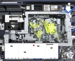
HMI e-beam metrology will deliver accurate patterning information, which ASML can use to optimize its powerful design and process models, a cornerstone of ASML’s successful computational lithography business. In return, those models can be used to guide the optical and e-beam metrology in a cost-effective manner to characterize the most relevant features on the chip device. Ultimately, this information combined with ASML modeling will provide the ability to adjust ASML’s scanners settings for optimal operation. Therefore, the transaction fits very well within ASML’s holistic lithography strategy.
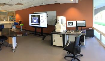
Furthermore, HMI has pioneered e-beam inspection systems that are specially designed for mask manufacturers to identify pattern defects in extreme ultraviolet (EUV) resulting from the mask. This will support the ramp of ASML’s EUV platform, set to be used for volume production of semiconductors starting in 2018.
The two companies are leaders in their respective fields and are already developing joint approaches that IC manufacturers can use to improve yields in the production of the most advanced microchips. The combination will allow ASML and HMI to further integrate and enhance their product offerings at an accelerated pace.
The integrated offerings will address the challenges chip makers are facing as they enter sub-10 nanometer resolutions and 3D integration, requiring chip manufacturers to apply advanced process control. This requires very dense, high-resolution metrology to measure and control device performance, whereas 3D integration requires very dense, high-voltage contrast metrology for process control.
Future customer requirements for better control of ever denser patterns at finer chip resolutions will drive product development of the integrated company for more advanced and faster e-beam systems. ASML and HMI expect that together they will be able to serve a significant portion of this fast-growing market.