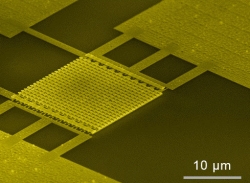
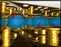
Engineers from the Applied Electromagnetics Group at the University of California San Diego report that they have fabricated the first semiconductor-free, optically controlled microelectronic device. Using metamaterials, engineers were able to build a microscale device that shows a 1000% increase in conductivity when activated by low voltage and a low-power laser.
The device consists of an engineered surface, called a metasurface, on top of a silicon wafer, with a layer of silicon dioxide in between. The metasurface consists of an array of gold mushroom-like nanostructures on an array of parallel gold strips. The gold metasurface is designed such that when a low DC voltage (under ten volts) and a low power infrared laser are both applied, the metasurface generates “hot spots”—spots with a high-intensity electric field—that provide enough energy to pull electrons out of the metal and liberate them into space. According to researchers, this particular metasurface was designed as a proof-of-concept. Different metasurfaces will need to be designed and optimized for different types of microelectronic devices.
“Next, we need to understand how far these devices can be scaled and the limits of their performance,” says electrical engineering professor and team leader Dan Sievenpiper. “This certainly won’t replace all semiconductor devices, but it may be the best approach for certain specialty applications, such as very high frequencies or high power devices.”
The team is also exploring other applications for this technology, such as photochemistry, photocatalysis, new kinds of photovoltaic devices, or environmental applications.
The discovery paves the way for microelectronic devices that are faster and capable of handling more power, and could also lead to more efficient solar panels. The work was published Nov. 4 in Nature Communications.
http://jacobsschool.ucsd.edu/news/news_releases/release.sfe?id=2060