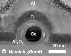
A team of scientists from the Nanoelectronic Materials Laboratory (NaMLab) and the Cluster of Excellence Center for Advancing Electronics Dresden at the Dresden University of Technology in Germany report that they have demonstrated the first germanium-based transistor that can be programmed between electron-(n) and hole-(p) conduction. Transistors based on germanium can be operated at low supply voltages and reduced power consumption, due to the low band gap compared to silicon. Additionally, germanium based transistors can be reconfigured between electron and hole conduction based on the voltage applied to one of the gate electrodes. This enables circuits with fewer transistors than state-of-the-art CMOS technologies.
For more than four decades, transistors have been miniaturized to enhance computational power and speed. Recent developments maintain this trend with materials having higher mobility than silicon in the transistor channel, such as germanium and indium arsenide. One of the limitations of these materials is the higher static power loss in the transistor´s off-state, also originating from their small band gaps.
The team succeeded in solving this issue by conceiving the germanium-nanowire transistor with independent gating regions. According to Dr. Walter Weber from NaMLab, “For the first time the results demonstrate the combination of low operating voltages with reduced off-state leakage. The results are a key enabler for novel energy efficient circuits.”
The work has been published in the journal ACS Nano.
http://www.namlab.de/news/press-release-namlab-02-17-ge-rfet-en.pdf?lang=en