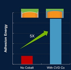
Applied Materials Inc., Santa Clara, Calif., announces a breakthrough in materials engineering in which cobalt replaces tungsten and copper for transistor contacts and interconnects. While challenging to integrate, cobalt brings significant benefits to chips and chip making: lower resistance and variability at small dimensions; improved gapfill at very fine dimensions; and improved reliability. Applied’s integrated cobalt suite is now shipping to foundry/logic customers worldwide.
Today, materials such as tungsten and copper are no longer scalable beyond the 10nm foundry node because their electrical performance has reached physical limits for transistor contacts and local interconnects. This has created a major bottleneck in achieving the full performance potential of FinFET transistors. Cobalt removes this bottleneck, but also requires a change in process system strategy. As the industry scales structures to extreme dimensions, the materials behave differently and must be systematically engineered at the atomic scale, often under vacuum.
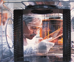
To enable the use of cobalt as a new conducting material in the transistor contact and interconnect, Applied has combined several materials engineering steps – pre-clean, PVD, ALD, and CVD – on the Endura platform. Moreover, Applied has defined an integrated cobalt suite that includes anneal on the Producer platform, planarization on the Reflexion LK Prime CMP platform, and e-beam inspection on the PROVision platform. Customers can use this proven, Integrated Materials Solution to speed time-to-market and increase chip performance at the 7nm foundry node and beyond.
“Five years ago, Applied anticipated an inflection in the transistor contact and interconnect, and we began developing an alternative materials solution that could take us beyond the 10nm node,” said Dr. Prabu Raja, senior vice president of Applied’s Semiconductor Products Group. “Applied brought together its experts in chemistry, physics, engineering, and data science to explore the broad portfolio of Applied’s technologies and create a breakthrough Integrated Materials Solution for the industry. As we enter the big data and AI era, there will be more of these inflections, and we will be having earlier and deeper collaborations with our customers to accelerate their roadmaps and enable devices we never dreamed possible.”