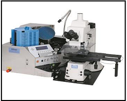
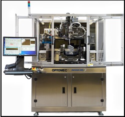
Nikon, Japan, introduces the NWL200 series, the first lineup of wafer loaders for inspection microscopes capable of loading 100-micron thin wafers. Thanks to a new chuck system, the NWL200 series achieves highly reliable loading suitable for inspection of next-generation semiconductors. Improved wafer-sensing functions also help prevent damage to wafers.
To prevent dust arising from friction or impact when centering the wafers, centering and alignment of the orientation flats and notches are completed without contact using photoelectric sensors. The system is configured so as not to interrupt the downflow of clean air into the clean room, and measures are taken to prevent particles on the suction surface of the wafer. In addition, the cover is stainless steel to prevent the build-up of static electricity and dust. Every measure has been taken to ensure that today’s highly integrated semiconductor production process is secure from contamination during inspection.
Should an error occur, an error message is displayed on the LCD panel. Even when the power is turned off, the vacuum chuck of the macro inspection mechanism stays on. If a problem occurs, wafers on the loader can be returned to the carrier without the use of tweezers.
https://www.nikonmetrology.com/en-gb/product/nwl200