 Researchers at the Department of Energy’s Lawrence Berkeley National Laboratory (Berkeley Lab), Berkeley, Calif., discover that electrons play a surprising role in heat transfer between layers of semiconductors, with implications for next-generation electronic devices.
As semiconductor devices become ever smaller, researchers are exploring two-dimensional (2D) materials for potential applications in transistors and optoelectronics. Controlling the flow of electricity and heat through these materials is key to their functionality, but first we need to understand the details of those behaviors at atomic scales.
Curious about how electrons and atomic vibrations couple to one another when heat flows between two materials, zooming into the interface with atomic precision allowed the researchers to uncover a surprisingly efficient mechanism for their coupling.
“Our work shows that we need to go beyond the analogy of Lego blocks to understand stacks of disparate 2D materials, even though the layers aren’t strongly bonded to one another,” said Archana Raja, a scientist at Berkeley Lab at who led the study. “The seemingly distinct layers, in fact, communicate through shared electronic pathways, allowing us to access and eventually design properties that are greater than the sum of the parts.”
In stacked layers of the 2D semiconductor materials tungsten diselenide (WSe2) and tungsten disulfide (WS2), researchers found that although they aren’t tightly bonded to one another, electrons provide a bridge between them that facilitates rapid heat transfer.
The devices were fabricated by Raja’s group at Berkeley Lab’s Molecular Foundry, who perfected the art of using Scotch tape to lift off crystalline monolayers of the semiconductors, each less than a nanometer in thickness. Using polymer stamps aligned under a home-built stacking microscope, these layers were deposited on top of each other and precisely placed over a microscopic window to enable the transmission of electrons through the sample.
In experiments conducted at the Department of Energy’s SLAC National Accelerator Laboratory, the team used ultrafast electron diffraction (UED) to measure the temperatures of the individual layers while optically exciting electrons in just the WSe2 layer. The UED served as an “electron camera”, capturing the atom positions within each layer. By varying the time interval between the excitation and probing pulses by trillionths of a second, they could track the changing temperature of each layer independently, using theoretical simulations to convert the observed atomic movements into temperatures.
The UED approach enables a new way of directly measuring temperature within this complex heterostructure. Aaron Lindenberg, a co-author on the study at Stanford University said “These layers are only a few angstroms apart, and yet we can selectively probe their response and, as a result of the time resolution, can probe at fundamental time scales how energy is shared between these structures in a new way.”
They found that the WSe2 layer heated up, as expected, but to their surprise, the WS2 layer also heated up in tandem, suggesting a rapid transfer of heat between layers. By contrast, when they didn’t excite electrons in the WSe2 and heated the heterostructure using a metal contact layer instead, the interface between WSe2 and WS2 transmitted heat very poorly, confirming previous reports.
“It was very surprising to see the two layers heat up almost simultaneously after photoexcitation and it motivated us to zero in on a deeper understanding of what was going on,” said Raja.
To understand their observations, the team employed theoretical calculations, using methods based on density functional theory to model how atoms and electrons behave in these systems with support from the Center for Computational Study of Excited-State Phenomena in Energy Materials (C2SEPEM), a DOE-funded Computational Materials Science Center at Berkeley Lab.
The researchers conducted extensive calculations of the electronic structure of layered 2D WSe2/WS2, as well as the behavior of lattice vibrations within the layers. Like squirrels traversing a forest canopy, who can run along paths defined by branches and occasionally jump between them, electrons in a material are limited to specific states and transitions (known as scattering), and knowledge of that electronic structure provides a guide to interpreting the experimental results.
Using computer simulations, the team explored where the electron in one layer initially wanted to scatter to, due to lattice vibrations. They found that electrons wanted to scatter to a hybrid state – a kind of ‘glue state’ where the electron hangs out in both layers at the same time. Now the team has a good idea of what these glue states look like and their signatures to confidently say that other, 2D semiconductor heterostructures will behave the same way.
The study appeared recently in Nature Nanotechnology.
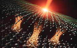
Image – Artistic depiction of electron transfer driven by an ultrashort laser pulse across an interface between two atomically-thin materials. This transfer is facilitated by an interlayer ‘bridge’ state that electrons are able to access due to lattice vibrations in both materials. Courtesy of: Gregory M. Stewart/SLAC.
For more information:
Lawrence Berkeley National Laboratory
U.S. Department of Energy’s Office of Science