Rigaku, Japan, leading provider of X-ray metrology solutions for semiconductor in-line processes, research and development, and high-volume manufacturing, has opened its first Semiconductor Metrology Technology Center in Sunnyvale, CA. The new facility has been established specifically to meet the needs of its semiconductor metrology tools clients and will showcase Rigaku’s latest thin film inspection, metrology, and monitoring technologies, as well as offering demonstrations, applications and operator training and maintenance services.
Rigaku has developed a wide portfolio of industry-leading semiconductor metrology and wafer inspection tools over the last 30 years, catering to everything from R&D to in-line fabrication. Establishing the new technology center will make these tools more accessible to the American semiconductor market and will foster closer working relationships between Rigaku and its clients, facilitating development of next-generation solutions.
At the new Rigaku Technology Center, visitors will experience the most reliable solutions for semiconductor metrology powered by the latest technology. These solutions will aid development of the next generation of devices, provide the highest throughput with compelling cost of ownership. Technologies include:
- TXRF (Total Reflection X-ray Fluorescence) – for detection of surface contamination
- WDXRF (Wavelength Dispersive X-ray Fluorescence) – for highly accurate and precise thickness and composition measurements
- Hybrid EDXRF (Energy Dispersive X-ray Fluorescence) and Optical Techniques – for characterization of multilayered samples, for BEOL and packaging applications, combining micro-spot EDXRF, with a 2D microscope, and 3D scanner for In-line non-destructive inspection and metrology, EDXRF (Energy Dispersive X-ray Fluorescence), XRR (X-ray Reflectivity), and XRD (X-ray Diffraction) – The combination of X-ray techniques supports a wide range of applications typically for the characterization of ultra-thin, multi-layer samples, blanket, and patterned samples.
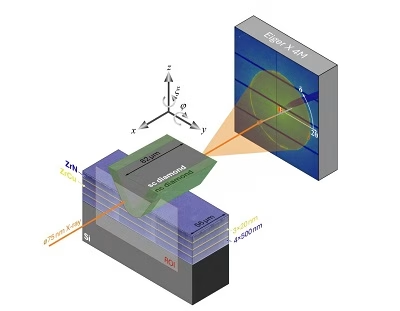
- HR-XRD (High-Resolution X-Ray Diffraction) and XRR – for strain, composition, and thickness of epitaxial layers, crystalline phase, and texture of polycrystalline films as well as thin film and film stack thicknesses and density.
Rigaku is constantly developing new technologies for non-destructive 3D measurement technology, semiconductor high-volume manufacturing process monitoring from lab to fab, metrology automation, thin film characterization, wafer contamination monitoring, and ultra-thin single-layer films to multi-layer stacks.
For more information:
Rigaku Semiconductor Metrology Division