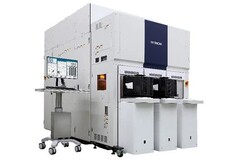
Hitachi High-Tech Corporation, Japan, launched the GT2000 high-precision electron beam metrology system to meet the needs of semiconductor device development and mass production in the high-NA EUV generation. The GT2000 uses Hitachi High-Tech’s technology and expertise in critical dimension-scanning electron microscope (CD-SEM), where it holds the top market share.
GT2000 is equipped with new detection systems to cutting-edge 3D semiconductor devices. It also utilizes low-damage high-speed multi-point measurement functions for High-NA EUV resist wafers imaging to minimize resist damage and improve yield in mass production.
The Hitachi High-Tech GT2000 CD-SEM will enable high-precision, high-speed measurements and inspection in the manufacturing process of advanced semiconductor devices, which are becoming increasingly miniaturized and complex, and contribute to the improvement of customer yields in research-and-development and mass production.
As semiconductor device manufacturing processes evolve, research-and-development of N2 (2-nanometer generation node) and A14 (14-angstrom generation node) is underway. In addition to the application of High-NA EUV lithography in state-of-the-art devices, the complexity of device structures is expected to increase, such as the gate all around (GAA) and complementary field effect transistor (CFET) structures.
Hence, the need for high-speed data acquisition under a wide range of measurement conditions to measure various materials and structures, stable operation and further tool-to-tool matching improvements in the research stages and mass production for cutting-edge semiconductor devices process development is increasing.
The GT2000 CD-SEM offers these key technologies:
1. 100V ultra-low acceleration voltage and ultra-high-speed multi-point measurement functionality for High-NA EUV processes
In the High-NA EUV lithography process, the resists used are thinner and, therefore, in order to measure it with high precision, metrology tool must cause as little damage as possible to the resist. GT2000 achieves low damage and high-precision measurement by combining pioneering ultra-low acceleration voltage of 100V, with our proprietary high-speed scanning functionality. In addition, it is equipped with an ultra-high-speed multi-point measurement mode to quickly determine manufacturing process conditions and detect abnormalities in research and development stage.
2. High-sensitivity detection system for 3D device structures
3D devices with structures such as GAA, CFET, and 3D memory require measurements of patterns’ depth, hole’ and trenches’ bottoms in addition to conventional CD measurement. GT2000 is equipped with a new highly sensitive detection system that efficiently detects backs-scattered electrons, enabling high-precision imaging of increasingly complex device structures and expanding the possibilities of new measurement applications.
3. New platforms and new electronic optical systems to improve tool-to-tool matching
One of the most important performance requirements for CD-SEM, which is responsible for process monitoring, is that the difference in measurement values between multiple tools is small. GT2000 new platform and electronic optical systems have been redesigned to eliminate any factors that cause differences in measurement values, thus, improving tool-to-tool matching.
For more information:
Hitachi High-Tech Corporation
https://www.hitachi-hightech.com/global/en/