Researchers at Nagoya University in Japan used artificial intelligence to discover a new method to understand dislocations in polycrystalline materials, materials widely used in information equipment, solar cells, and electronic devices, that can reduce the efficiency of such devices. The findings were published in the journal Advanced Materials.
Almost every device that we use in our modern lives has a polycrystalline component but these materials are tough to use because of their complex structure. Along with their composition, the performance of a polycrystalline material is affected by its complex microstructure, dislocations, and impurities.
A major problem for using polycrystals in industry is the formation of the tiny crystal defects caused by stress and temperature changes known as dislocations. They can disrupt the regular arrangement of atoms in the lattice, affecting electrical conduction and overall performance. To reduce the chances of failure in devices that use polycrystalline materials, it is important to understand the formation of these dislocations.
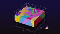
The team used new AI to analyze image data of polycrystalline silicon. The AI created a 3D model in virtual space, helping the team to identify the areas where dislocation clusters were affecting the material’s performance.
After identifying the areas of the dislocation clusters, the researchers used electron microscopy and theoretical calculations to understand how these areas formed. They revealed stress distribution in the crystal lattice and found staircase-like structures at the boundaries between the crystal grains. These structures appear to cause dislocations during crystal growth.
“We found a special nanostructure in the crystals associated with dislocations in polycrystalline structures,” said Professor Noritaka Usami who led the research.
Along with its practical implications, this study may have important implications for the science of crystal growth and deformation as well. The Haasen-Alexander-Sumino (HAS) model is an influential theoretical framework used to understand the behavior of dislocations in materials. But Usami believes that they have discovered dislocations that the Haasen-Alexander-Sumino model missed.
The team was also surprised when calculations of the arrangement of the atoms in these structures revealed unexpectedly large tensile bond strains along the edge of the staircase-like structures that triggered dislocation generation.
“As experts who have been studying this for years, we were amazed and excited to finally see proof of the presence of dislocations in these structures. It suggests that we can control the formation of dislocation clusters by controlling the direction in which the boundary spreads,” Usami explained.
“By extracting and analyzing the nanoscale regions through polycrystalline materials informatics, which combines experiment, theory, and AI, we made this clarification of phenomena in complex polycrystalline materials possible for the first time,” Usami continued.
“This research illuminates the path towards establishing universal guidelines for high-performance materials and is expected to contribute to the creation of innovative polycrystalline materials. The potential impact of this research extends beyond solar cells to everything from ceramics to semiconductors. Polycrystalline materials are widely used in society, and the improved performance of these materials has the potential to revolutionize society.”
Top image: Researchers used 3D model created by AI to understand complex polycrystalline materials that are used in our everyday electronic devices. Courtesy of: Kenta Yamakoshi.
For more information:
Nagoya University