

Universal Scientific Industrial (Shanghai) Co., Ltd., China, developed an advanced electronic component failure analysis technology to meet the increasingly complex and diverse needs of system-in-package miniaturized products.
Continue readingNew surface coating technology increases materials’ electron emission seven-fold
An international research group with researchers from China, Japan, and the Los Alamos National Laboratory, Los Alamos, NM, developed a new surface coating technology that is capable of significantly increasing electron emission in materials.
Continue readingGeorgia Tech and GlobalFoundries to collaborate on joint semiconductor research and workforce development
Georgia Institute of Technology, Atlanta, one of the top public research universities in the U.S., and GlobalFoundries, Malta, NY., one of the world’s leading semiconductor manufacturers, announced a new partnership to expand collaboration on semiconductor research, education, talent, and workforce development.
Continue readingA step forward in the quest to replace silicon with 2D chips
Researchers at The University of Texas at Austin have discovered more than a dozen different materials for 2D semiconductors that could allow electrons to quickly move around, opening the door for a leap in electronics’ capabilities.
Continue readingStacking LEDs instead of placing them side by side could enable fully immersive virtual reality displays
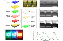 MIT engineers, Boston, Mass., have developed a new way to make sharper, defect-free displays, stacking the diodes to create vertical, multicolored pixels. Each stacked pixel can generate the full commercial range of colors and measures about 4 microns wide. The microscopic pixels, or micro-LEDs, can be packed to a density of 5,000 pixels per inch.
Over the years, the size of individual pixels has shrunk, enabling many more of them to be packed into devices to produce sharper, higher-resolution digital displays. But LEDs are reaching a limit to how small they can be while also performing effectively, especially noticeable in close-range displays such as augmented and virtual reality devices, where limited pixel density results in a “screen door effect” such that users perceive stripes in the space between pixels.
“This is the smallest micro-LED pixel, and the highest pixel density reported in the journals,” says Jeehwan Kim, associate professor of mechanical engineering at MIT. “We show that vertical pixellation is the way to go for higher-resolution displays in a smaller footprint.”
For next-generation displays, researchers are exploring inorganic micro-LEDs—diodes that are one-hundredth the size of conventional LEDs and are made from inorganic, single-crystalline semiconducting materials. Micro-LEDs could perform better, require less energy, and last longer than OLEDs.
Typical micro-LED fabrication using pick-and-place has required extreme accuracy, as microscopic pixels of red, green, and blue need to first be grown separately on wafers then precisely placed on a plate, in exact alignment with each other in order to properly reflect and produce various colors and shades. Achieving such microscopic precision is a difficult task, and entire devices need to be scrapped if pixels are found to be out of place.
The new MIT technique using vertical arrangement is an entirely different potentially less wasteful way to fabricate micro-LEDs.
The research group previously developed a method to grow and peel away perfect, two-dimensional, single-crystalline material from wafers of silicon and other surfaces—an approach they call 2D material-based layer transfer, or 2DLT.
In the current study, this approach was used to grow ultrathin membranes of red, green, and blue LEDs. They then peeled the entire LED membranes away from their base wafers, and stacked them together to make a layer cake of red, green, and blue membranes. They could then carve the cake into patterns of tiny, vertical pixels, each as small as 4 microns wide.
“In conventional displays, each R, G, and B pixel is arranged laterally, which limits how small you can create each pixel,” Shin says. “Because we are stacking all three pixels vertically, in theory we could reduce the pixel area by a third.”
The team has shown that it can grow, peel, and stack ultrathin LEDs. As a demonstration, the team fabricated a vertical LED pixel, and showed that by altering the voltage applied to each of the pixel’s red, green, and blue membranes, they could produce various colors in a single pixel.
“If you have a higher current to red, and weaker to blue, the pixel would appear pink, and so on,” Shin says. “We’re able to create all the mixed colors, and our display can cover close to the commercial color space that’s available.”
The team plans to improve the operation of the vertical pixels. So far, they have shown they can stimulate an individual structure to produce the full spectrum of colors. They will work toward making an array of many vertical micro-LED pixels.
“You need a system to control 25 million LEDs separately,” Shin says. “Here, we’ve only partially demonstrated that. The active matrix operation is something we’ll need to further develop.”
Results are published in the journal Nature.
Image – Vertically stacked, full-color µLEDs enabled by 2DLT. Courtesy of: Nature (2023).
For more information:
Massachusetts Institute of Technology