Materials scientists at Rice University, Houston, Texas, have developed a new workflow methodology for measuring microscopic defects in diamond and other advanced semiconductor materials. By making it easier to spot flaws that can undermine performance, the approach could accelerate the development of more reliable electronic and quantum devices.
The research team developed a custom Python-based software tool to rapidly analyze data from high-resolution X-ray diffraction, a technique that uses X-rays to probe a material’s internal crystal structure. The software analyzes the resulting diffraction patterns, picks up on dislocations and irregularities in the atomic lattice, and calculates their density in a given material.
“Dislocations can disrupt how charge and heat move through the material, which impacts how efficient and reliable a device is and how easy it is to manufacture at scale,” said Xiang Zhang, assistant research professor of materials science and nanoengineering at Rice and a corresponding author on the study published in Advanced Materials.
This framework is particularly suited for wide-bandgap semiconductors like diamond, which are increasingly vital for high-power electronics and quantum technologies due to their ability to handle extreme heat and electrical stress.
“Diamond is emerging as a key material for future high-power electronics, radio-frequency communication and quantum technologies because it can tolerate high heat and extreme electrical conditions better than many conventional semiconductors,” said Tia Gray, a Rice doctoral alumna and first author on the study who now works as a National Research Council postdoctoral associate with the U.S. Naval Research Laboratory. “However, its performance depends strongly on crystal quality.”
For manufacturers and researchers alike, measuring crystal quality has remained a persistent challenge. Existing approaches can be time-consuming, difficult to scale or dependent on labor-intensive analysis. While similar X-ray-based methods have been widely used for other semiconductor materials, applying them to diamond has proven more difficult because diamond’s crystal structure and defect behavior differ from those of more commonly studied materials.
To test the new framework, the researchers analyzed four commercially available grades of single-crystal diamond with different expected levels of crystal quality. The automated workflow clearly distinguished among the materials, identifying electronic-grade diamond as having the lowest defect density and most uniform crystal quality. Heteroepitaxial diamond, which is grown on a nondiamond substrate, exhibited the highest defect density and greatest structural disorder.
Different techniques used to validate the results showed consistent trends, supporting the reliability of the approach.
The team also applied the workflow to gallium nitride, another advanced semiconductor used in power electronics and radio-frequency devices, demonstrating that the approach can be adapted across different crystal structures and growth platforms.
The researchers plan to continue refining the methodology and expand the range of materials and defect types it can analyze.
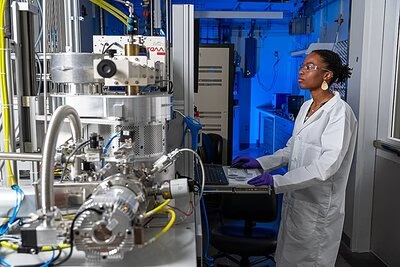
Image – Tia Gray, a Rice doctoral alumna who now works as a National Research Council postdoctoral associate with the U.S. Naval Research Laboratory is the first author on a study published in Advanced Materials. Courtesy of: Brandon Martin/Rice University.
For more information:
https://www.rice.edu/