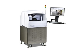
Bruker Nanosurfaces Division, Billerica, Mass., introduces the Dektak XTL Stylus Profiler, extending its stylus profilometry capabilities to 200 and 300 mm semiconductor wafer fabs and next-generation touch panel manufacturers. The system provides the most cost-effective, full 300-mm wafer solution for characterizing thin film step heights, resist step heights, line edge roughness, CMP dishing, erosion, and roll off amount (ROA).
The Dektak XTL combines decades of stylus innovation with new features targeting QA/QC environments to enable increased accuracy and minimal operator intervention between loading and unloading samples.
It features a small footprint with pneumatic passive isolation and a fully enclosed workstation with a wide, easily accessible interlocking door, making it suitable for demanding production floor environments. Its dual-camera architecture enables enhanced spatial awareness, and its high level of automation maximizes manufacturing throughput. Bruker’s exclusive Vision64 Advanced Production Interface (API) with pattern recognition optimizes the system for stringent QA/QC requirements and makes data collection an intuitive and repeatable process, minimizing operator-to-operator variability.
“Bruker’s Dektak XTL with a 12-inch stage is the most advanced system in its class,” said Roger Lee, Integration Department Project Director for China Wafer Level CSP Co., Ltd. (WLCSP). “The system is stable and reliable, and it incorporates many powerful functionalities and ease-of-use features. Bruker’s stylus profilers always lead the industry in technology, and they always meet our metrology requirements in production.”