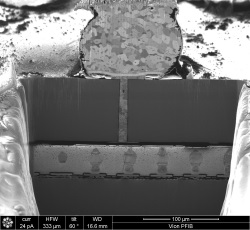
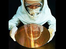
FEI Corp., Hillsboro, Ore., offers the Helios PFIB for large area deprocessing to enable electrical fault isolation of advanced process ICs, and advanced failure analysis of 3D packages. It is the said to be the world’s most advanced DualBeam Plasma FIB platform for large area sample preparation and analysis in semiconductor failure analysis, process development, and process control laboratories.
The system combines the innovative Helios Elstar with UC technology electron column for high-resolution, high-contrast imaging, with the high-performance Vion Xenon plasma ion column for fast and precise large area sample cross-sectioning and deprocessing. Combined with FEI’s proprietary Si Trenching, Dx and DE chemistries offer a unique deprocess/delayering solution for electrical fault isolation in the latest process technology devices.
The Helios PFIB DualBeam features FEI’s most recent advances in plasma-focused ion beam and field emission SEM technologies and their combined use. FEI’s first plasma-based DualBeam is designed for high throughput, large volume processing, combined with extreme high-resolution imaging in both 2D and 3D. For large scale cross-sectioning, large volume 3D data collection, or large scale patterning, the instrument provides the highest quality of data in the shortest time.