Kansas State University, Manhattan, reports that its researchers have developed a better way to build semiconductors and layer them to minimize potential defects. Dr. James Edgar, University Distinguished Professor of chemical engineering, has received a patent for his invention, “Off-axis silicon carbide substrates,” which results in substrates with fewer defects.
The research may help improve electronic devices and could benefit the power electronics industry and manufacturers of semiconductor devices. Electronics are made of semiconductors crystals that must be layered perfectly for the electronic device to work.
“It’s like a stacked cake separated by layers of icing,” says Prof. Edgar. “When the layers of semiconductors don’t match up very well, it introduces defects. Any time there is a defect, it degrades the efficiency of the device.”
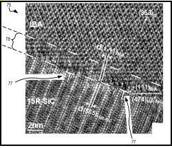
Prof. Edgar describes the research discovery as serendipitous. Several years ago, when Yi Zhang, a 2011 doctoral graduate in chemical engineering, was working in the laboratory, she found a substrate sample that was very smooth. Collaborative researchers at the State University of New York at Stony Brook, and the University of Bristol in the United Kingdom, later confirmed the layer’s presence and proved that it had fewer defects than on the standard substrate.
“We have applied this process to other systems,” Prof. Edgar says. “We are working on verifying that it is not just these specific materials we started with, but that it can be applied to a lot of different materials.”