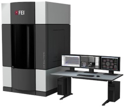
FEI, Hillsboro, Ore., introduces the DualBeam plasma-focused ion beam (PFIB) for sample preparation, electrical fault isolation, and electrical failure analysis on sub-20nm semiconductor devices. The system combines FEI’s high-performance plasma ion column, proprietary Dx de-processing, and Elstar UC low kV SEM technology to provide damage-free accurate end-pointing down to the transistor contact layer. Many of the other Helios platform options and features are also available on the PFIB EFI, including silicon trenching, delineation etch chemistries, infrared/visible light microscope, and analytical capabilities such as EBSD and EDX.
“Semiconductor process development and yield enhancement engineers no longer need to tolerate delays due to a multi-tool, multi-operator approach to electrical fault isolation and failure analysis,” says Rob Krueger, vice president and general manager of FEI’s semiconductor business.
“The new Helios PFIB EFI is a fully integrated, easy-to-use solution that reduces the number of steps and sample transfers during the process. Eliminating these bottlenecks helps to reduce the process debug and device analysis cycle time by 50% to 80%, and improve yields to near 100%, enabling chip makers to achieve significantly faster time-to-volume manufacturing.”
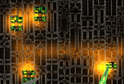
The Helios PFIB EFI is built upon the world’s most advanced DualBeam Plasma FIB platform with fully-integrated SEM and nanoprobing capabilities, delivering site-specific sample preparation with in-situ SEM end-pointing and low-beam energy SEM-based transistor characterization. It includes electron-beam absorbed current (EBAC) for interconnect-level electrical fault isolation, and electron-beam induced current (EBIC) analysis for diffusion characterization. The system boosts deprocessing yields for 10nm devices by using FEI’s unique Dx delayering solution.
www.fei.com/helios-pfib-efi-for-electronics