Akhan Semiconductor, Gurnee, Ill., has opened its global headquarters and production facility to develop and manufacture next-generation diamond-based semiconductors. Its breakthrough Miraj Diamond portfolio is combined with low-temperature diamond deposition technology developed by Argonne National Laboratory’s Center for Nanoscale Materials.
According to the company, diamond-based semiconductors can operate at temperatures of over 300°C, reducing the costs required for cooling systems and overheating-related repairs. They can handle ten times higher voltages, allowing new technologies to utilize higher power without more material. They can operate with over 90% better power efficiency by reducing the ambient power loss compared to current technology.
Diamond’s ability to conduct heat far surpasses that of materials used on current electronics (five times better than copper, 22 times better than silicon). It also has the unique ability to isolate massive voltages with a small fraction of the material required compared to present technologies. In isolating 10,000 volts, the amount of diamond needed is 50 times less than that of silicon.
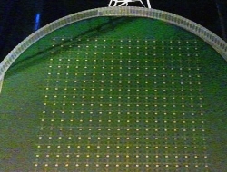
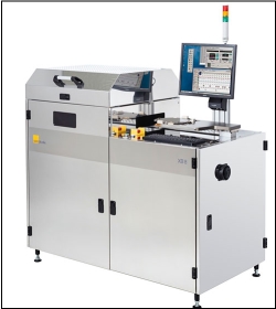
The company has developed a state-of-the-art manufacturing process that takes common methane gas as the input, and produces the perfect diamond wafers needed for electronic production. At a basic level, the process is to crack the methane gas onto a heated platform using a ball of plasma. Methane and hydrogen plasma are exposed to microwave energy to form very thin diamond materials over various sizes and thicknesses. They can be formed on a variety of materials such as silicon, sapphire, and glass, among others. The final product is a diamond wafer that can serve as a platform for fabricating semiconductor devices.