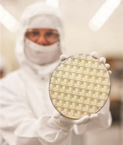
Imec, Belgium, announces the opening of its new 4000-square-meter cleanroom facility dedicated to scaling IC technology beyond 7nm, bringing the total floor space of its semiconductor research cleanrooms to 12,000 square meters.
Extending the existing cleanroom, the new facility complies with the newest standards in the semiconductor industry, and provides additional space for the most advanced tools that will lead innovations in new device and system concepts. Installations of the first tools began in January 2016. The new 300mm cleanroom complements Imec’s other production facilities, including its bio-nanolabs, neuroelectronics labs, imaging-wireless-electronics test labs, photovoltaic pilot lines, and GaN-on-Si, silicon photonics, and MEMS pilot lines.
“Since our founding in 1984, Imec has become the world’s largest independent nanoelectronics research center with the highest industry commitment,” stated Luc Van den hove, president and CEO at Imec. “This success is the result of the unique combination of our broad international partner network, including the major global players of the semiconductor industry, top scientific and engineering talent, and imec’s one of a kind infrastructure. The extension of our cleanroom provides our partners with the necessary resources for continued leading edge innovation and imec’s success in the future within the local and global high-tech industry.”
The new cleanroom comprises a total investment (building and equipment) of more than $1.1 billion, of which $112 million was from the Flemish Government and more than $1 billion consists of investments from joint R&D with the leading players from the entire semiconductor industry, totaling more than 90 industrial partners.