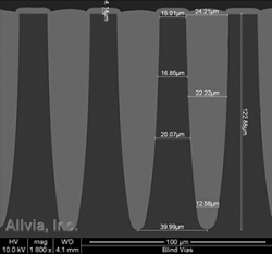
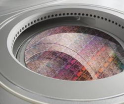
Allvia, Sunnyvale, Calif., has expanded its capacity for glass and quartz via manufacturing to accommodate customer requests in via-fill technology from silicon interposers to glass and quartz interposers. This will enable next-generation semiconductor 2D and 2.5D packaging solutions using ultra-thin glass and quartz.
The company’s goal is to commercialize the widespread use of interposers. The company will expand its intellectual property from silicon to glass in hole drilling and filling methodologies to fabricate its interposers.
Allvia will apply its proprietary technology to fill the high-aspect-ratio via holes with copper plating. Its processes and its production line can produce all types of interposers to achieve the next generation in high-density semiconductor packaging. These 2D and 2.5D interposers are needed to form the electrical connections between a silicon chip and PCBs.
According to Sergey Savastiouk, CEO, “Our expansion allows us to solve two problems. First, we become more flexible with customer requests; second, we can produce more wafers with better quality using state-of-the-art for copper plating, chemical mechanical polishing, and deep via thin film deposition.”
Allvia provides Silicon and Glass Interposer and Through-Silicon Via (TSV) and TGV foundry services to Semiconductor, Optoelectronics and MEMS industries, to meet the demands of advanced vertical interconnects, 2.5D, 3D, and System-in-Package (SiP) solutions.
A leader in TSV development, Allvia provides design and processing for frontside (filled) and backside (conformal plated) through-silicon vias. With its full line of in-house processing equipment, it offers services for prototyping as well as volume production runs.