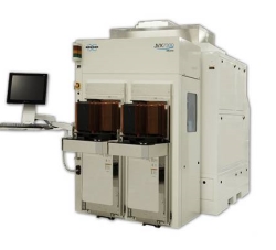
Bruker Corp., Billerica, Mass., Germany, announces that multiple leading logic and foundry manufacturers have selected Bruker’s JVX7300LSI X-ray metrology system to support their ramp and development for 10 nm and 7/5 nm technology nodes. The tool supports a wide range of X-ray metrology modes to provide solutions for a large variety of materials and structures. It is capable of measuring the composition, thickness, and strain/relaxation of single and multiple epilayer stacks using both large-spot and small-spot HRXRD.
The tool is equipped with both large and small spot measurement capabilities for in-line production process monitoring of the most advanced logic devices. The tool was selected by manufacturers following a comprehensive evaluation of extremely challenging measurements across a variety of front-end applications, including SiGe and Ge epitaxial analysis on Si and SRB, finFETs and (FD)SOI, III-V, and other materials such as high-k/metal gate characterization.
“We are delighted to have been selected by industry-leading semiconductor customers to provide an unparalleled metrology solution for advanced epitaxial processes,” said David V. Rossi, President of the Bruker Semiconductor Division. “Strengthening our position in fab-based X-ray metrology was part of the rationale behind Bruker’s acquisition of Jordan Valley Semiconductors in 2015, and we view this selection as further proof of our technology leadership as a provider of advanced X-ray based solutions.”