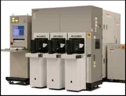
Hitachi High-Technologies Corp., Japan, launches its Advanced High Voltage CD-SEM – CV5000 Series, which is capable of measuring high aspect-ratio trenches and contact holes, as well as measuring device patterns.
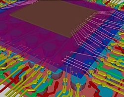
Recent efforts to enhance performance of advanced semiconductor devices include not only miniaturization, but also advances in three-dimensional reconstruction. The mainstream architecture of a semiconductor device now is a stack of multiple elements arranged vertically, especially in 3D-NAND flash-memory chips, Fin-FET logic transistors, and VIT interconnects.
During the manufacturing process, high precision is more necessary than ever for measurement of the bottom dimensions of deep trenches and contact holes. Moreover, the overlay alignment precision of each layer has also become very important.
The newly launched CV5000 series is fitted with a 30 kV electron gun and a detection system that is capable of detecting secondary electrons and backscattered electrons emitted from a sample based on emission angle and energy. This detection system enables the tool to measure at the bottom of deep trenches and contact holes with aspect ratios of more than 40 on advanced devices, and high-precision overlay measurements of the device patterns.
The special mark necessary for conventional optical overlay measurement is not used, although Hitachi High-Tech enables the products to measure device patterns directly with a high-acceleration electron beam. This measurement method improves the overlay alignment precision of the device patterns, either on the same layers or different layers.
The CV5000 series will be introduced at Semicon Japan 2016 at Tokyo Big Sight from December 14 to 16, 2016.