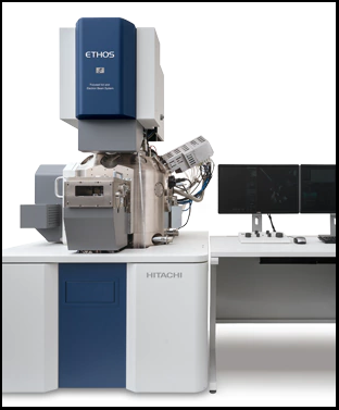
Hitachi High-Technologies Corp., Tokyo, announces the development of an all-new high-performance Ethos FIB-SEM based on a newly developed magnetic/electrostatic compound lens that enables it to deliver advanced imaging performance resolving sub-nanometer features in high contrast for low-voltage SEM applications.
The EthosS FIB-SEM system incorporates a FIB column used in sample preparation along with the newest SEM concept for high-magnification observation, enabling the analysis of microscopic surface structure and topography at micron scale.
The system is designed to play an important role especially in the fields of high-performance devices and nanomaterials, where miniaturization has been advancing recently, for the preparation of uniformly thin, high-grade TEM samples for observation and analysis of fine structure at atomic resolution levels, as well as for defect analysis and evaluation.
Ethos incorporates world-class Hitachi High-Tech core technologies in the form of a high-intensity cold-cathode field emission electron gun combined with the newly developed magnetic/electrostatic compound lens for high-resolution imaging at low acceleration voltages, along with real-time FIB process observation capabilities.
Combined with Anti-Curtaining Effect (ACE) technologies that suppress curtaining effects or striations during cross-section sample preparation. In addition, Ethos is capable of preparing high-grade, quality TEM samples uniformly in its triple-beam configuration. The electron system is also equipped with multiple detectors to separate selective high-contrast or topographic electrons from secondary electrons, ensuring no structural details at the nanometer scale are missed.
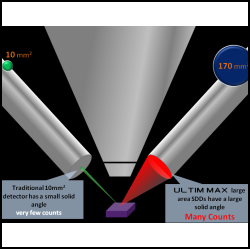
The system is designed with an innovative large-volume sample chamber equipped with ports for Energy Dispersive X-ray Spectrometer (EDS) and Electron Backscatter Diffraction (EBSD), along with a multitude of additional analytical detection configurations possible with optimum detector positioning. The sample chamber is designed for users who are prepared for customization and upgradeability in the future. Samples can be processed and observed from all angles with a large 155-mm X-Y stage. Design considerations for the modern scientists in every field delivers ETHOS for looking at not only the latest semiconductors, but also everything from biological samples to magnetic materials such as steel.
Similar to Hitachi’s FIB-SEM lineup such as the NX2000 which launched in September 2014 and the NX9000 which launched in June 2015, ETHOS has been co-developed by Hitachi High-Tech with its wholly owned subsidiary Hitachi High-Tech Science Corporation. Sales are due to commence in fall 2017.
Hitachi High-Technologies will continue to promote development and sales expansion of highly sophisticated solutions and technologies by responding swiftly to the needs of customers and markets, working from the customer’s perspective as a fast-moving creator of cutting-edge businesses.