Akhan Semiconductor, Gurnee, Ill., a developer of diamond semiconductor technology, announces that it is deploying 200mm manufacturing equipment and process in its new production facility in Gurnee. This continues its preparation for delivering diamond-based semiconductor technology products to the company’s first commercial customer this quarter.
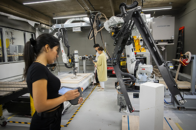
“The proven, high-yielding 200mm semiconductor manufacturing process is proving ideal for the production of a wide range of semiconductors – sensors, MEMS, analog, power management – that are embedded in the rapidly growing number of connected devices, from smartphones and tablets to cars, home appliances, wearables, and commercial and industrial applications,” says Akhan COO Carl Shurboff.
According to market research firm Gartner Inc., the number of Internet-connected devices, now referred to as the Internet of Things, will grow from 6.3 billion in 2016 to more than 20 billion in 2020.
This explosion in connected products is driving high global demand for all types of new semiconductors to power this new era of connected computing. SEMI noted in its Global 200mm Fab Outlook to 2018, that 200mm fab capacity is expected to grow from 5.2 million wafer starts per month in 2015 to more than 5.4 million in 2018.
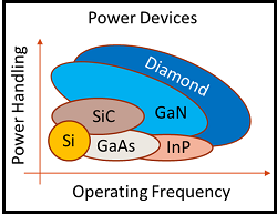
“The timing for our diamond-based semiconductor technology’s market debut could not be better,” says Akhan CEO Adam Khan. “By using man-made diamonds at the core of our new chip technology, we are ushering in a new generation of semiconductor solutions that operate at higher temperatures, are thinner, and require less power. These are exactly the attributes required for all the products that make up the Internet of Things.”
Akhan’s technology is based on a new process in which man-made diamond rather than silicon produces new chip materials. It is a result of the marriage of two scientific breakthroughs: the ability to use nanocrystalline diamond (NCD) films and a new doping process the makes it possible to use NCD as a semiconductor material.