Upping its commitment to its state-of-the-art wafer fab in Arizona, Taiwan Semiconductor Manufacturing Corp. (TSMC), Taiwan, is reported to be investing some $35 billion in the U.S. manufacturing facility, almost tripling the original $12 billion it originally committed.
TSMC said in May of last year construction on the Arizona facility was planned to begin in 2021 with production slated to begin in 2024, and that it would be capable of producing 20,000 300 mm semiconductor wafers per month. The $12 billion investment would be used through 2029 and the facility would create more than 1,600 jobs directly and thousands of indirect jobs in the ecosystem.
According to Taiwanese newspaper United Daily News, TSMC will expand its plans for the Arizona facility into a gigafab capable of producing 100,000 wafers per month. Additionally, the report indicates TSMC will offer salaries to Taiwan-based employees to move to Arizona.
While the move to build a fab in the U.S. happened prior to the COVID-19 pandemic, the move comes at a time when capacity is tight in all semiconductor areas leading to a crippling automotive chip shortage, which could last all year. While building more fabs will not solve this short-term issue because it takes years to get a fab up and running, the gigafab will be able to handle the anticipated 5% growth over the next decade for semiconductor manufacturing, leading to a boom in fab construction.
According to the Semiconductor Industry Association (SIA), the share of global semiconductor manufacturing capacity in the U.S. has decreased from 37% in 1990 to 12% today. This decline is due to subsidies offered by foreign governments, which have placed the U.S. at a competitive disadvantage in attracting new fab construction, the SIA said.
The expansion of the TSMC facility will also contribute to a renewed interest in expanding domestic U.S. semiconductor manufacturing, which has become a major issue for U.S. semiconductor companies, trade organizations and the U.S. government.
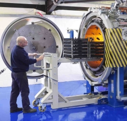
Image – A TSMC worker develops 300mm wafers at a facility in Taiwan. The company plans to spend more on its 300mm wafer fab it plans to build Arizona based on future semiconductor demand. Courtesy of TSMC.
For more information:
TSMC
https://www.tsmc.com/english