A team lead by researchers at the Royal Melbourne Institute of Technology (RMIT), Australia, introduced ultrathin beta-tellurite to the 2D semiconducting material family, providing an answer to the decades-long search for a high mobility p-type oxide.
A new study, published in Nature Electronics, could pave the way to revolutionary, transparent electronics. Such see-through devices could potentially be integrated in glass, in flexible displays, and in smart contact lenses, bringing to life futuristic devices that seem like the product of science fiction.
For several decades, researchers have sought a new class of electronics based on semiconducting oxides, whose optical transparency could enable fully-transparent electronics. Oxide-based devices could also find use in power electronics and communication technology, reducing the carbon footprint of our utility networks.
A barrier to oxide devices has been that while many high-performance n-type oxides are known, there is a significant lack of high-quality p-type oxides. But, in 2018, a computational study revealed that beta-tellurite (β-TeO2) could be an attractive p-type oxide candidate with tellurium’s place in the periodic table indicating it can behave as both a metal and a non-metal, providing its oxide with uniquely useful properties.
“This prediction encouraged our group at RMIT University to explore its properties and applications. This new, high-mobility p-type oxide fills a crucial gap in the materials spectrum to enable fast, transparent circuits,” says team leader Dr. Torben Daeneke, who led the collaboration with three Future Low-Energy Electronics Technologies (FLEET) partners at RMIT.
Dr. Daeneke’s team demonstrated the isolation of beta-tellurite with a specifically developed synthesis technique that relies on liquid metal chemistry. The process is similar to drawing, using a glass rod as a pen and liquid metal as ink.
While the desirable β-phase of tellurite grows below 300°C, pure tellurium has a high melting point, above 500°C. Selenium was added to design an alloy that has a lower melting point, making the synthesis possible.
A molten mixture of tellurium (Te) and selenium (Se) was prepared and allowed to roll over a surface. Due to oxygen in the ambient air, the molten droplet naturally forms a thin surface oxide layer of beta-tellurite. As the liquid droplet is rolled over the surface, this oxide layer sticks to it, depositing atomically thin oxide sheets in its way.
The 1.5 nanometer thick ultrathin sheets with a bandgap of 3.7 eV were highly transparent across the visible spectrum, essentially invisible to the human eye.
To assess the electronic properties of the developed materials, field-effect transistors were fabricated. The devices showed characteristic p-type switching as well as a high hole mobility (roughly 140 cm2V-1s-1), showing that beta-tellurite is ten to one hundred times faster than existing p-type oxide semiconductors. The excellent on/off ratio (over 106) also attests the material is suitable for power efficient, fast devices.
The findings, fast, transparent p-type semiconductors, have the potential to revolutionize transparent electronics while enabling better displays and improved energy-efficient devices, closing a crucial gap in the electronic material library.
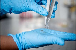
Image – The optical transparency of the new materials could enable futuristic, flexible, transparent electronics. Courtesy of RMIT University.
For more information:
RMIT University
https://www.rmit.edu.au/