Achieving the auto industry’s stringent zero-defect goals is becoming a big challenge for makers of silicon carbide substrates, which are struggling to achieve sufficient yields and reliability as they migrate from 150 to 200 mm wafers and shift their focus away from pure silicon.
SiC is a combination of silicon and harder carbide materials, and it has emerged as a key technology for battery electric vehicles due to its wide bandgap. Silicon carbide works at higher power, higher temperatures, and higher switching frequencies than silicon. Those properties can be leveraged to increase the range of EV batteries and shorten the charging time.
“People want to charge their car in under 10 to 15 minutes, and that will continue to evolve,” said Sam Geha, CEO of Infineon Technologies’ Memory Solutions. “That will require silicon carbide and other technologies, and a lot more automation.”
There is no shortage of companies rushing to fill this void, as evidenced by recent investments. Last month, onsemi announced a deal to buy GT Advanced Technologies’ SiC technology for $415 million. Likewise, STMicroelectronics bought Norstel AB in 2019 for $137.5 million (total value; ST already owned 55%). In addition, Cree announced in 2019 that it would build a $1.2 billion 200mm SiC fab in Marcy, N.Y., with production scheduled to start next year.
Silicon carbide is in high demand for a variety of applications, particularly in the automotive sector where it is ideal for electric vehicle power conversion chips due to the high breakdown field strength, thermal conductivity and efficiency.
Common testing today include high magnification inline optical analysis to detect defects, statistical analysis of electrical parameters, and pattern analysis of wafer maps. In some cases, further physical analysis such as chemical delayering and focused ion beam analysis (FIB) may be required.
Other techniques like x-ray diffraction (XRD) also are being deployed for SiC. XRD is used to characterize crystalline materials. Deployed in the industry for years, XRD first made inroads in the semiconductor industry for logic. It was, and still is, used to characterize silicon germanium materials in devices. Over time, XRD has moved to other areas. “It has been added to the compound side, like for gallium-nitride. We have a big market for high-performance LEDs and III-V materials,” said Paul Ryan, vice president and general manager of the X-ray Business Unit at Bruker. “The next big up and comer is silicon carbide, looking at the quality on that either with straight diffraction or diffraction imaging.”
In addition, tools that locate and map defects on SiC wafers are commercially available and are typically based on UV irradiation of the wafer. This mapping, with defect type and impact criteria, determines the wafer’s usable area.
Inspection tools have to keep pace with a variety of changes as new materials are introduced and used in both planar and complex heterogeneous packages.
KLA and Lasertec sell inspection systems for SiC. These tools combine two technologies—surface defect inspection and photoluminescence metrology. Photoluminescence is a non-contact spectroscopy technique, which looks at the crystal structures of devices. Reducing the defectivity rate has an economic benefit, too, and one way to tackle that is through well-controlled epitaxy.
“Today, major players have the know-how and experience to optimize their epitaxies to avoid critical defects propagating through the epilayer stack,” Yole’s Ben Slimane said. “At the process level, the gate oxide is one of the main challenges for SiC devices which can result in shorter lifetime devices. High-temperature burning tests are essential to optimize this step and avoid this problem. Besides, SiC is not CMOS-compatible, making it challenging to leverage Si technology processes as well as the infrastructure and requires investments to adapt existing fabs or build new ones.”
But the processes to identify and control defects still need some work.
Some of this is due to a shift to larger wafer sizes, and by way of comparison, the ramp from 200mm to 300mm for bulk silicon was difficult. This is compounded by the fact that SiC is being used increasingly in safety-critical applications, where defects can result in injury or death. Also in automotive applications, carmakers are demanding that chips function to spec for as long as 18 years and there is extreme pressure to reduce costs by improving yield.
All of this will take time, but the market outlook is strong. So from a business standpoint, there is strong incentive to solve these issues quickly, and no shortage of companies looking to do that.
Many silicon fabs are starting to process SiC wafers, as well, and given the plethora of 200mm Si fabs with fully depreciated tools, there are a lot of large 200mm fabs/foundries waiting on the sidelines to enter SiC production when 200 mm wafers become available.
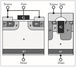
Image – Planar-gate MOSFET (left) and trench MOSFET (right). Courtesy of: Infineon
For more information:
original article on Semi Engineering
https://semiengineering.com/inspecting-testing-and-measuring-sic/
Bruker
Cree
Infineon Technologies
KLA Tencor
Lasertec
https://www.lasertec.co.jp/en/
onsemi
STMicroelectronics
Yole