Researchers at the Berkeley Lab Molecular Foundry report that they have developed rhenium disulfide, a semiconductor that functions electronically as if it were a 2D monolayer even as a 3D bulk material. This opens the door to 2D electronic applications with a 3D material, and makes it possible to study 2D physics with easy-to-make 3D crystals.
“Rhenium disulfide remains a direct-bandgap semiconductor, its photoluminescence intensity increases while its Raman spectrum remains unchanged, even with the addition of increasing numbers of layers,” says Junqiao Wu, a physicist with Berkeley Lab’s Materials Sciences Division who led this discovery. “This makes bulk crystals of rhenium disulfide an ideal platform for probing 2D excitonic and lattice physics, circumventing the challenge of preparing large-area, single-crystal monolayers.”
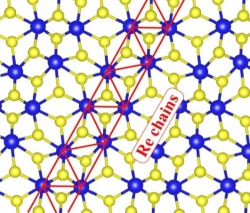
Dr. Wu, who is also a professor with the University of California-Berkeley’s Department of Materials Science and Engineering, headed a large international team of collaborators who used the facilities at the Molecular Foundry, a U.S Department of Energy (DOE) national nanoscience center, to prepare and characterize individual monolayers of rhenium disulfide. Through a variety of spectroscopy techniques, they studied these monolayers both as stacked multilayers and as bulk materials. Their study revealed that the uniqueness of rhenium disulfide stems from a disruption in its crystal lattice symmetry called a Peierls distortion.
“Semiconducting transition metal dichalcogenides consist of monolayers held together by weak forces,” says Sefaattin Tongay, lead author of a paper describing this research in Nature Communications for which Wu was the corresponding author. The paper was titled “Monolayer behaviour in bulk ReS2 due to electronic and vibrational decoupling.”