A team of IBM researchers in Switzerland with support from colleagues in Yorktown Heights, N.Y. has developed a relatively simple, robust and versatile process for growing crystals made from compound semiconductor materials that will allow them be integrated onto silicon wafers—an important step toward making future computer chips that will allow integrated circuits to continue shrinking in size and cost even as they increase in performance.
The work may allow an extension to Moore’s Law, the famous observation by Gordon Moore that the number of transistors on an integrated circuit double about every two years. In recent years some in the industry have speculated that our ability to keep pace with Moore’s Law may become exhausted eventually unless new technologies come along that will lend it leash.
“The whole semiconductor industry wants to keep Moore’s Law going. We need better performing transistors as we continue down-scaling, and transistors based on silicon won’t give us improvements anymore,” says Heinz Schmid, a researcher at IBM.
For consumers, extending Moore’s Law will mean continuing the trend of new computer devices having increasing speed and bandwidth at reduced power consumption and cost. The new technique may also impact photonics on silicon, with active photonic components integrated seamlessly with electronics for greater functionality.
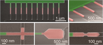
The team fabricated single crystal nanostructures, such as nanowires, nanostructures containing constrictions, and cross junctions, as well as 3D stacked nanowires, made with so-called III–V materials. Made from alloys of indium, gallium and arsenide, III-V semiconductors are seen as a possible future material for computer chips, but only if they can be successfully integrated onto silicon. So far efforts at integration have not been very successful.
The new crystals were grown using an approach called template-assisted selective epitaxy (TASE) using metal organic chemical vapor deposition, which basically starts from a small area and evolves into a much larger, defect-free crystal. This approach allowed them to lithographically define oxide templates and fill them via epitaxy, in the end making nanowires, cross junctions, nanostructures containing constrictions and 3D stacked nanowires using the already established scaled processes of Si technology.
“What sets this work apart from other methods is that the compound semiconductor does not contain detrimental defects, and that the process is fully compatible with current chip fabrication technology,” says Schmid. “Importantly the method is also economically viable.”
He added that more development will be required to achieve the same control over performance in III-V devices as currently exists for silicon. But the new method is the key to actually integrating the stacked materials on the silicon platform, Schmid says.
Image caption — SEM images of single crystal structures fabricated using template-assisted selective epitaxy. For better visibility, silicon is colored in green, and the compound semiconductor in red.