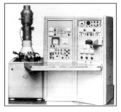
Carl Zeiss Microscopy Ltd., England, marked the 50th anniversary of the first sale of a commercial scanning electron microscope with an event in Cambridge. Customers and specialists from many disciplines had the chance to meet scientists who worked on its development. Between 1951 and 1961, a team of engineering PhD students led by Sir Charles Oatley built the world’s first five SEMs. In 1965, they built the first commercial SEM, the StereoScan (photo), with the Cambridge Instrument Company, a Zeiss predecessor.
With 50 years of continuous growth and development, the SEM has become ever more versatile, and is now firmly established as an indispensable tool for advanced research across many scientific disciplines. With new industrial applications emerging every year, the SEM is also a vital part of research & development, and quality control and analysis across an extensive range of industries.
From its early home in materials science, the SEM established itself in the disciplines of electronics, forensics, and archaeology. Over the years it has evolved into a key tool for food technologists, biologists, geologists and petrologists in the natural resources industries, adapting to fulfill the discrete requirements of these individual applications. Use of SEMs for process control and failure analysis is now widespread, with routine analysis on SEMs an integral part of the semiconductor and automotive industries, and manufacture more broadly.
Development still goes on: A direct descendant of the first microscopes produced in Cambridge in 1965 is the ZEISS EVO family. First launched in 2004, and widely accepted as the industry leading analytical platform, there are some developments soon to be unveiled for EVO offering more flexibility, ease of use, and further development of detectors. The new ZEISS Gemini SEM family comes with a novel optical design. Users achieve better resolution, especially at low voltage. With 20 times greater in-lens detection signal, they always acquire crisp images fast and with minimum sample damage.
http://www.photonics.com/Article.aspx?AID=20667
http://www.zeiss.com/semiconductor-manufacturing-technology/en_de/news-events.html