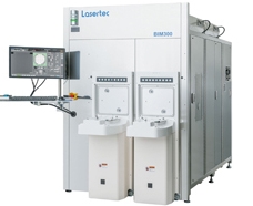
Lasertec, Japan, offers the WASAVI series BIM300 laser microscope, which achieves high-resolution observation on wafer surfaces, as well as high precision measurement of via reveal and bump dimensions and shapes. The instrument combines a high-precision XY stage with Lasertec’s core technologies accumulated through many years of experience with industrial laser microscopes.
BIM300 is a useful inspection and measurement tool that facilitates bump forming process optimization, wafer periphery inspection, and wafer grinding process optimization. The measurement of through glass via (TGV) plating patterns is another application where BIM300 can be used effectively.
In 3D device manufacturing process, it is necessary to maintain via reveal, bump dimensions and bump shapes on wafer surface as uniform as possible for stable bonding between layers.
In order to increase production yield, it is important to be able to accurately measure the height, diameter and shape of each bump to help control these parameters. Although bumps have been used for some time, today’s most advanced 3D devices use much smaller bumps than before, and it is necessary to measure bump dimensions in about 0.1µm accuracy.
In 3D device manufacturing, it is also necessary to grind each wafer much thinner than the conventional wafer to keep the distance between layers as short as possible. This will facilitate high integration to ensure low energy consumption and high speed. Grinding wafers thinner, however, increases the risk of cracked or broken chips in wafer’s peripheries. It is therefore important to have the capability to inspect the peripheries of ground wafers for process control purposes.
www.lasertec.co.jp