Suny Polytechnic Institute, Utica, N.Y., and Global Foundries, Milpitas, Calif., have established a new Advanced Patterning and Productivity Center, a $500 million, five-year program to accelerate the introduction of extreme ultraviolet lithography technologies into manufacturing. The center will be located at the Colleges of Nanoscale Science and Engineering in Albany, N.Y. It is anchored by a network of international chipmakers and material and equipment suppliers, including IBM and Tokyo Electron, and will generate 100 jobs.
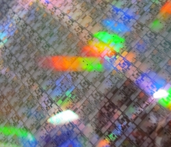
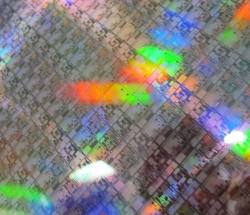
EUV lithography is a next-generation semiconductor manufacturing technique that produces short wavelengths of light (14-nanometers and below) to create minuscule patterns on integrated circuits. The technology is critical to achieving the cost, performance, and power improvements needed to meet the industry’s anticipated demands in cloud computing, Big Data, mobile devices, and other emerging technologies.
A key component of the center will be the installation of the ASML NXE:3300 EUV scanner, a state-of-the-art tool for the development and manufacturing of semiconductor process technologies at 7nm and beyond. This installation follows the installation of the IBM supported ASML NXE:3300B EUV scanner already in place at Suny Poly.
The center aims to bring mask and materials suppliers together to extend the capabilities of EUV lithography through exploring fundamental aspects of the patterning process. Other projects will be focused on enhancing productivity, in preparation for implementing EUV lithography in the manufacturing of leading-edge products in Global Foundries’ production facility in Malta, N.Y.
Through the APPC, members will have access to Suny Poly’s patterning infrastructure, which includes state-of-the-art film deposition and etch capability, leading-edge patterning systems, EUV mask infrastructure, and world-class EUV imaging capabilities.