Designing a 3D-printed structure is hard enough when the product is inches or feet in size. Imagine shrinking it smaller than a drop of water, smaller even than a human hair, until it is dwarfed by a common bacterium.
This impossibly small structure can be made a reality with focused electron beam induced deposition, or FEBID, to essentially 3D print at the nanoscale. FEBID uses an electron beam from a scanning electron microscope to condense gaseous precursor molecules into a solid deposit on a surface.
Previously, this method was laborious, prone to errors, and impractical for creating complex structures larger than a few nanometers. Now, a team at the DOE’s Oak Ridge National Laboratory, Tenn., in collaboration with the University of Tennessee and the Graz University of Technology, developed a powerful simulation-guided drafting process to improve FEBID and introduce new possibilities in nanomanufacturing.
Team leader Jason Fowlkes, a research staff member at ORNL’s Center for Nanophase Materials Sciences says the new system integrates design and construction into one streamlined process that creates complex 3D nanostructures.
He also notes the ability to accurately design custom nanostructures “opens up a host of novel applications in 3D plasmonics, free-standing nanosensors and nanomechanical elements on the lower nanoscale which are almost impossible to fabricate by other techniques.”
The process uses a 3D simulation to guide the electron beam and replicate complex lattices and meshes between 10 nm and 1 μm in size. The model tracks electron scattering paths and the release of secondary electrons to predict the pattern of deposition on the surface of the material and visualize the final structure of an experiment.
The innovative aspect of this work, according to Fowlkes, is the convergence of experiments and simulation. Simulation guides the experimental construction, while the completed experiments, in turn, provide feedback on the accuracy and strength of the simulation. Designs are fed into the simulation and drafting program, and any inconsistencies between the two caused by secondary electron activity can be caught before the experiment.
“In its simplest form, once we know the emission profile of those secondary electrons we don’t want, we can design around them,” Fowlkes says.
While slower than other nanofabrication methods available in the clean room at CNMS, the FEBID process is the only one that can produce high-fidelity 3D nanostructures, Fowlkes says. With no way to “see” the nanostructures during construction, researchers previously relied on trial and error, manually adjusting the build parameters to produce the desired shapes.
The team will now focus on fully purifying the structures of carbon contamination. The purification process, called in situ purification, removes the impurities during construction, using water or oxygen and a laser to liberate the residual carbon from the precursor and flush it out of the structure. The simulation can even incorporate the stresses of the carbon removal process and can anticipate the transformation in the final product.
“We can design structures in a way where the actual writing pattern might look distorted, but that’s taking into account the fact that it’s going to retract and contract during purification and then it will look like the proper structure,” Fowlkes says.
ORNL is managed by UT-Battelle for the Department of Energy’s Office of Science, the single largest supporter of basic research in the physical sciences in the United States. DOE’s Office of Science is working to address some of the most pressing challenges of our time.
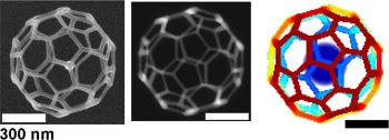
Image caption — 32-face 3D truncated icosahedron mesh was created to test the simulation’s ability to precisely construct complex geometries. The SEM image of the final experimental product (left) was highly consistent with the structure predicted by the virtual SEM image (center) and the simulated design model (right).