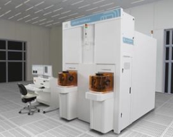
Applied Materials Inc., Santa Clara, Calif., announces that its next-generation ProVision e-beam wafer inspection system delivers the highest resolution and image quality at the fastest throughput, to foundry, logic, DRAM and 3D NAND customers as they move to advanced nodes.
The ProVision system is said to be the only e-beam hotspot inspection with one nanometer resolution. This allows customers to detect the most challenging “killer” defects that other technologies cannot find, and to monitor process marginality to rapidly resolve ramp issues and achieve higher yields.
Offering three times faster throughput over existing e-beam hotspot inspection tools, the system ensures accurate process characterization, prediction, and detection of performance defects and yield-limiting defects throughout the fab product life cycle. It complements Applied’s e-beam metrology and review products, as well as the optical patterned wafer inspection product line.
The ProVision system is gaining momentum with already more than a dozen shipments, including repeat orders from a leading foundry and a major memory manufacturer. Additional systems are scheduled for shipment to existing and new customers in the second half of 2016.