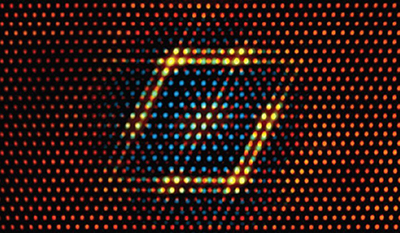
Imec, Belgium, has shown for the first time that a silicon-passivated germanium nMOS gate stack with reduced interface defect density reaches the same defect level as a silicon gate stack, and has high mobility with reduced positive bias temperature instability. These results pave the way for germanium-based finFETs and gate all-around devices, as promising options for 5-nm and beyond logic devices.
Reduced defects were achieved by band engineering using an interface dipole at high-k/SiO2 interface, and a hydrogen high-pressure anneal finalizing the process flow. The interface dipole was formed on the SiO2 layer by depositing a lanthanum SiO film via atomic layer deposition, which is a 3D-compatible process.
While a high interface defect density has been the leading concern for Si-passivated Ge nFET, it was dramatically reduced for the first time, from 2×1012 cm-2eV-1, down to 5×1010 cm-2eV-1 around midgap, by using a combination of the LaSiO insertion and a hydrogen high-pressure anneal. Consequently, electron mobility was increased by ~50% at peak, while PBTI reliability was improved, thanks to the interface dipole-induced band engineering.
This work was done in collaboration with ASM, Poongsan, and Nanyang Technological University. Imec’s research into advanced logic scaling is performed in cooperation with imec’s key partners in its core CMOS programs, including Globa lFoundries, Huawei, Intel, Micron, Qualcomm, Samsung, SK Hynix, Sony and TSMC.