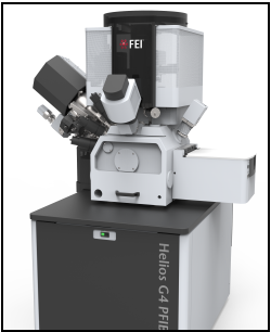
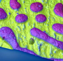
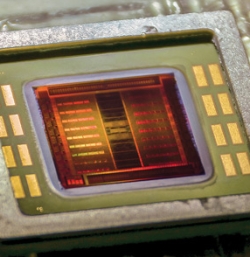
Thermo Fisher Scientific, Hillsboro, Ore., announces three new additions to its portfolio of semiconductor failure analysis workflows. The Helios G4 plasma-focused ion beam system is designed to deprocess and provide ultra-high-resolution SEM analysis on a wide variety of semiconductor devices. The flexProber system enables fast electrical fault isolation to identify and locate faults at both the interconnect and the transistor levels of the semiconductor wafer. The Themis S transmission electron microscope provides atomic-level resolution imaging and high-throughput chemical analysis on the most challenging semiconductor devices.
The Helios G4 plasma FIB system is Thermo Fisher's latest-generation DualBeam microscope. It can perform a wide variety of failure analysis applications, from high-speed delayering to SEM cross-section imaging of devices and TEM sample preparation. Semiconductor delayering is an increasingly important application in fault localization at sub-14nm technology nodes. The plasma FIB and proprietary Dx chemistry is used to expose metallization layers, allowing electrical fault isolation and analysis to be performed with Thermo Fisher nanoprobing tools.
The Helios G4 plasma FIB system can support deprocessing down to the 7nm node and offers automated end pointing that stops milling automatically when the metal or via layer of interest is exposed. It provides up to 10-20 times faster milling rates than conventional (Ga+) FIB solutions, allowing engineers to create larger samples for nanoprobing and TEM imaging, as well as large area SEM cross-sections, on a broad range of advanced (2.5D) packaging, light-emitting diode (LED), display and microelectromechanical systems (MEMS).
The new flexProber system is designed to help engineers to quickly locate and identify electrical faults, using an SEM to position fine mechanical probes on exposed circuit elements. Accurately locating the fault can improve productivity and cost-effectiveness in subsequent analysis by ensuring that the fault is included when a thin section is extracted for high-resolution imaging in a TEM. The flexProber system includes a new SEM column specifically designed for probing applications, with a 2X improvement in resolution compared to its predecessor, the nProber II. It incorporates many of the capabilities of Thermo Fisher's high-end Nanoprober product line and is designed to address a broad range of semiconductor device types and process technologies. It provides an ideal pathway into electrical probing, offering an entry-level configuration while preserving the option to upgrade to full Nanoprober system capability in the future.
The Themis S system is Thermo Fisher's latest addition to the industry-standard Themis TEM platform. Targeted at the needs of semiconductor failure analysis labs working at the sub-20nm technology node, the Themis S system is designed for high-volume semiconductor imaging and analysis and includes an integrated vibration isolation enclosure and full remote operation capability. The probe-corrected, 80-200kV column, automated alignments, XFEG source and DualX x-ray spectrometer provide robust, sub-Ångström imaging and fast, accurate elemental and strain analysis.