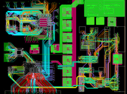
Advanced Semiconductor Engineering Inc., Taiwan, and Cadence Design Systems Inc., San Jose, Calif., announce that they have collaborated to release a System-in-Package (SiP) EDA solution that addresses the challenges of designing and verifying Fan-Out Chip-on-substrate multi-die packages.
The solution consists of the SiP-id (System-in-Package – intelligent design) design kit, an enhanced reference flow including IC packaging and verification tools from Cadence, and a new methodology that aggregates the requirements of wafer-, package-, and system-level design into a unified and automated flow. By deploying the SiP-id methodology, designers can reduce design iterations and greatly improve throughput as compared to existing advanced packaging EDA tools, reducing the time needed to design and verify ultra-complex SiP packages.
Previously, IC packaging engineers leveraged standard EDA design tools coupled with a set of loosely defined rules to lay out their packages. However, this approach has many limitations when designing today’s advanced multi-die packages. To provide a more holistic approach to the design and verification of SiP and advanced fan- out packages, ASE and Cadence collaborated closely to develop a design kit, methodology, and streamlined and automated reference flow using enhanced Cadence® IC packaging and verification tools, all tailored for ASE’s advanced IC package technologies. In a typical use case with high-pin-count dies, packaging engineers using SiP-id and the accompanying reference flow and methodology were able to reduce time from more than six hours to only 17 minutes, compared to existing tools with manual operation.
www.aseglobal.com/en/Technology/AdvancedTechnology.asp