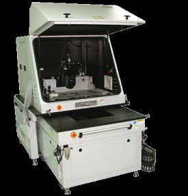
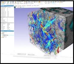
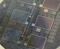
Semicaps Corp. Ltd., Singapore, offers the Semicaps scanning optical microscope for fault localization of integrated circuits using laser-induced phenomena. It is an integrated compucentric system designed for maximum ease of use and flexibility. The system is optimized for high laser-power delivery, sensitivity, and spatial resolution. The open architecture of the system allows the application of current and future laser-induced techniques.
The modular design facilitates customization according to user requirements. Semicaps offers two types of scanning optical microscope configuration for industrial use: the analytical (upright/inverted) and the tester docked (inverted) systems. The systems are designed for OBIC, SCOBIC, LIVA, TIVA, SEI, OBIRCH, and pulsed laser technique and are upgradable for future techniques.
The system uses a 1064nm and a 1340nm laser. The 1064nm laser is capable of electron-hole pair generation through backside silicon, while the 1340nm laser is a high resolution thermal probe which allows localized heating. The laser multiplexer provides seamless selection, attenuation, and blanking of the two lasers.
The Semicaps microscope module is custom designed to provide maximum flexibility for the optical components required for various techniques. Included in the microscope module is a motorized detector selector, a pair of three-position optical component turrets, and a five-position objective turret. The system comes with an auxiliary signal port, which has a proprietary hardware averager capable of one million sample averaging.
The standard system uses two near-IR lasers. The 1064nm laser is capable of efficient electron-hole pair generation through backside silicon, while the 1340nm laser is a high-resolution thermal probe that allows localized heating. The laser multiplexer provides seamless selection, attenuation, and pulsing of the lasers. Additional laser can be integrated into the system.
https://www.semicaps.com/som.htm